
Methods And Systems For Determining Quality Of Semiconductor Measurements

Active Publication Date: 2022-03-24
KLA TENCOR CORP
View PDF5 Cites 0 Cited by
  • Summary
  • Abstract
  • Description
  • Claims
  • Application Information

AI Technical Summary

Benefits of technology

This patent describes a method for measuring parameters in a close proximity to a target, to better identify changes in process parameters that may be required. The measurement results can also be used to provide active feedback to the process tool. The technical effects include improved process control and optimization, better quality of products, and increased efficiency in the manufacturing process.

Problems solved by technology

In most cases, the raw measurement signals cannot be used to directly determine the physical properties of the specimen.
For example, measurement data outside the domain of the measurement data observed during the model training phase may give rise to large prediction errors due to extrapolation.
Unfortunately, these traditional techniques have met with limited practical success.
Thus, ensemble mean prediction fails to accurately estimate measurement uncertainty and fails to directly measure the quality of the measurement model.
In addition, Bayesian regression and bootstrap sampling are computationally expensive and practically unsuitable for implementation as part of a high volume semiconductor fabrication facility.
Finally, the aforementioned techniques are not normalized.
Without normalization, the results cannot be consistently interpreted across different measurement recipes or structures under measurement.
Future metrology applications present challenges for metrology due to increasingly small resolution requirements, multi-parameter correlation, increasingly complex geometric structures, and increasing use of opaque materials.

Method used


Image

  • Methods And Systems For Determining Quality Of Semiconductor Measurements
  • Methods And Systems For Determining Quality Of Semiconductor Measurements
  • Methods And Systems For Determining Quality Of Semiconductor Measurements

Examples


Embodiment Construction

[0035]Reference will now be made in detail to background examples and some embodiments of the invention, examples of which are illustrated in the accompanying drawings.

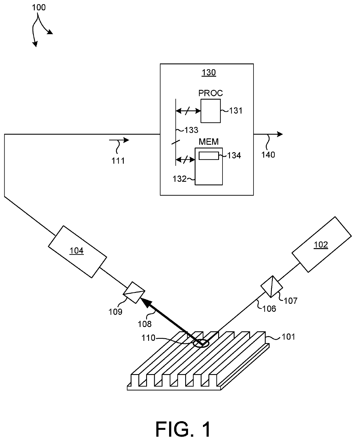
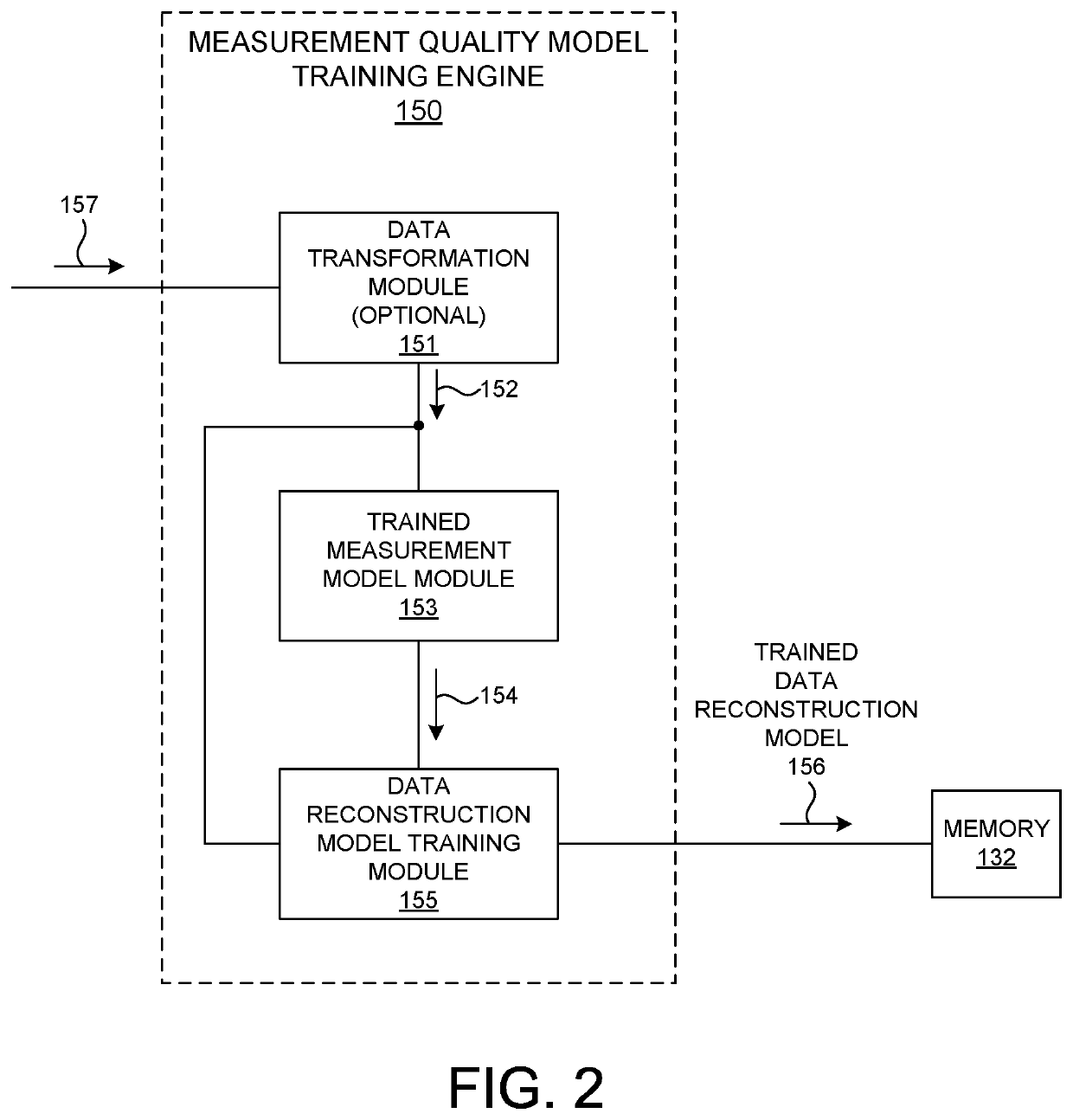
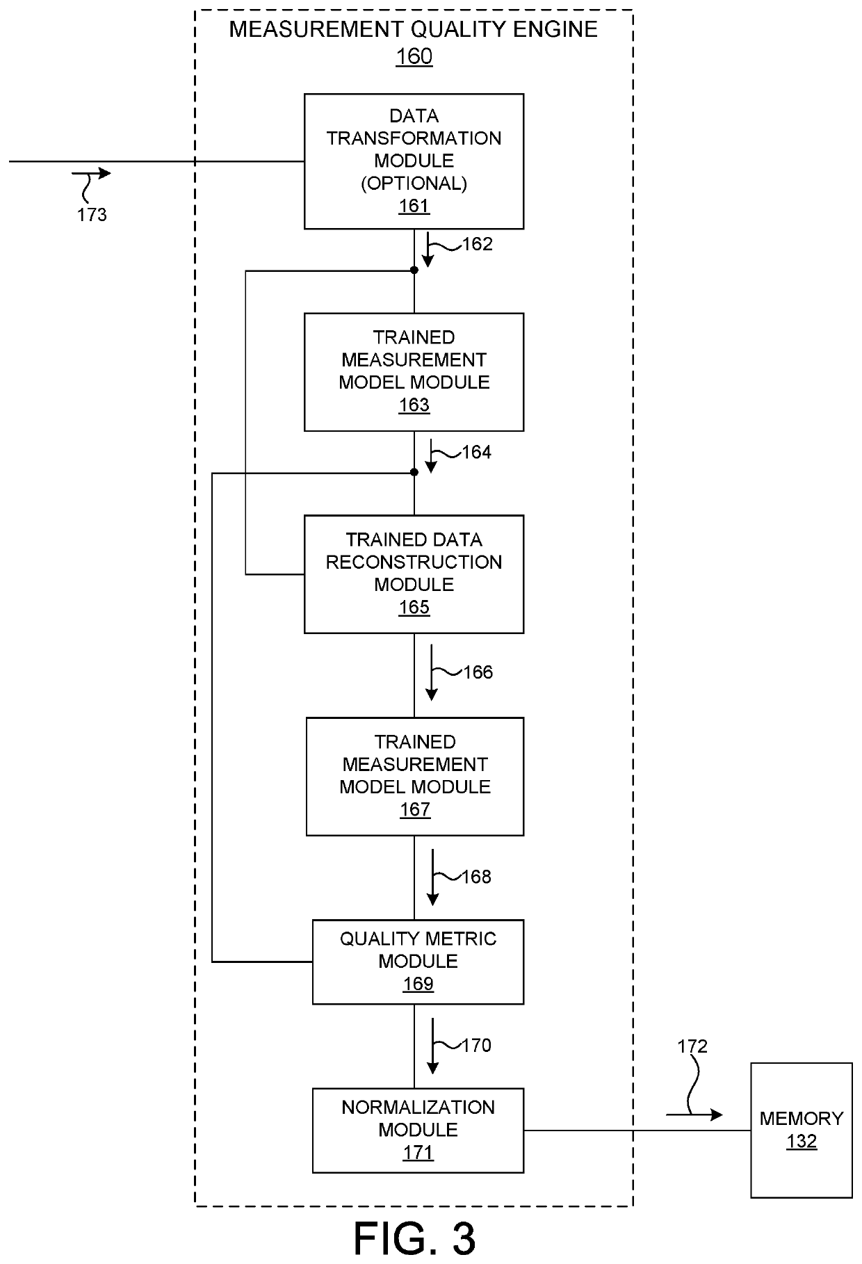
[0036]Methods and systems for estimating a value of a quality metric indicative of one or more performance characteristics of a semiconductor measurement are presented herein. A quality metric is determined from a quality metric model trained based on actual measurement data, simulated measurement data, or both, and reference measurement data. Once trained, the quality metric model enables the calculation of a quantitative quality metric indicative of measurement quality for a particular measurement recipe based on measurement data collected from inline wafers at each measurement site without using reference metrology. The value of the quality metric is normalized to ensure applicability across a broad range of measurement scenarios.

[0037]In general, the value of a quality metric is indicative of measurement uncertain...


PUM


Abstract

Methods and systems for estimating a value of a quality metric indicative of one or more performance characteristics of a semiconductor measurement are presented herein. The value of the quality metric is normalized to ensure applicability across a broad range of measurement scenarios. In some embodiments, a value of a quality metric is determined for each measurement sample during measurement inference. In some embodiments, a trained quality metric model is employed to determine the uncertainty of defect classification. In some embodiments, a trained quality metric model is employed to determine the uncertainty of estimated parameters of interest, such as geometric, dispersion, process, and electrical parameters. In some examples, a quality metric is employed as a filter to detect measurement outliers. In some other examples, a quality metric is employed as a trigger to adjust a semiconductor process.

Description

TECHNICAL FIELD[0001]The described embodiments relate to metrology systems and methods, and more particularly to methods and systems for improved measurement of semiconductor structures.BACKGROUND INFORMATION[0002]Semiconductor devices such as logic and memory devices are typically fabricated by a sequence of processing steps applied to a specimen. The various features and multiple structural levels of the semiconductor devices are formed by these processing steps. For example, lithography among others is one semiconductor fabrication process that involves generating a pattern on a semiconductor wafer. Additional examples of semiconductor fabrication processes include, but are not limited to, chemical-mechanical polishing, etch, deposition, and ion implantation. Multiple semiconductor devices may be fabricated on a single semiconductor wafer and then separated into individual semiconductor devices.[0003]Metrology processes are used at various steps during a semiconductor manufacturi...

Claims


Application Information

Patent Timeline
IPC IPC(8): G01B11/25G01B15/04
CPCG01B11/25G01B15/04G01B21/045G01B2210/56G01B11/02G01B15/02G01N2021/8883G01N21/274G03F7/70616
Inventor SANKO, DZMITRYMOON, MIN-YEONGPANDEV, STILIAN IVANOV
Owner KLA TENCOR CORP
Learn More