Semiconductor device
a technology of semiconductors and devices, applied in the direction of solid-state devices, transistors, high-frequency amplifiers, etc., can solve the problem that such hbts cannot have a sufficient breakdown tolerance (load change breakdown tolerance), and achieve the effect of improving load change breakdown tolerance and thermal stability
- Summary
- Abstract
- Description
- Claims
- Application Information
AI Technical Summary
Benefits of technology
Problems solved by technology
Method used
Image

Examples
first working example
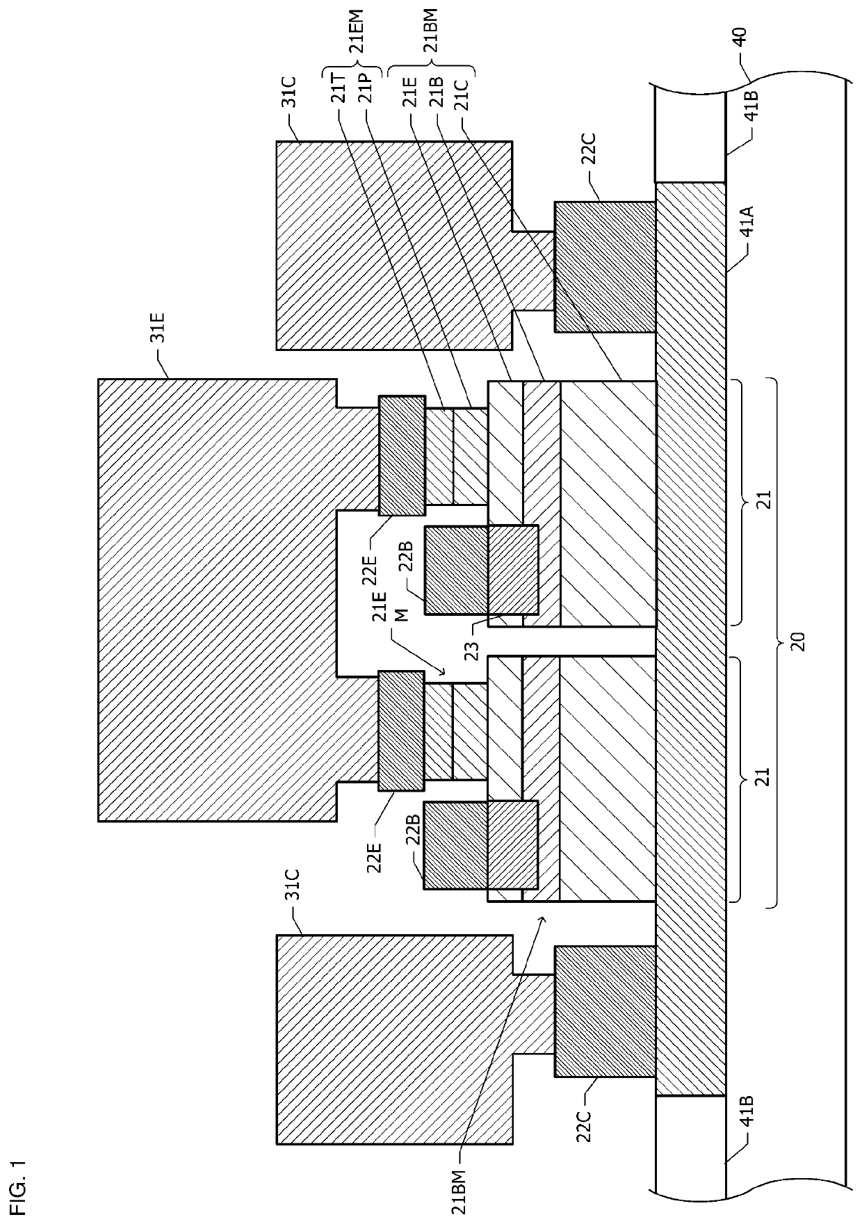
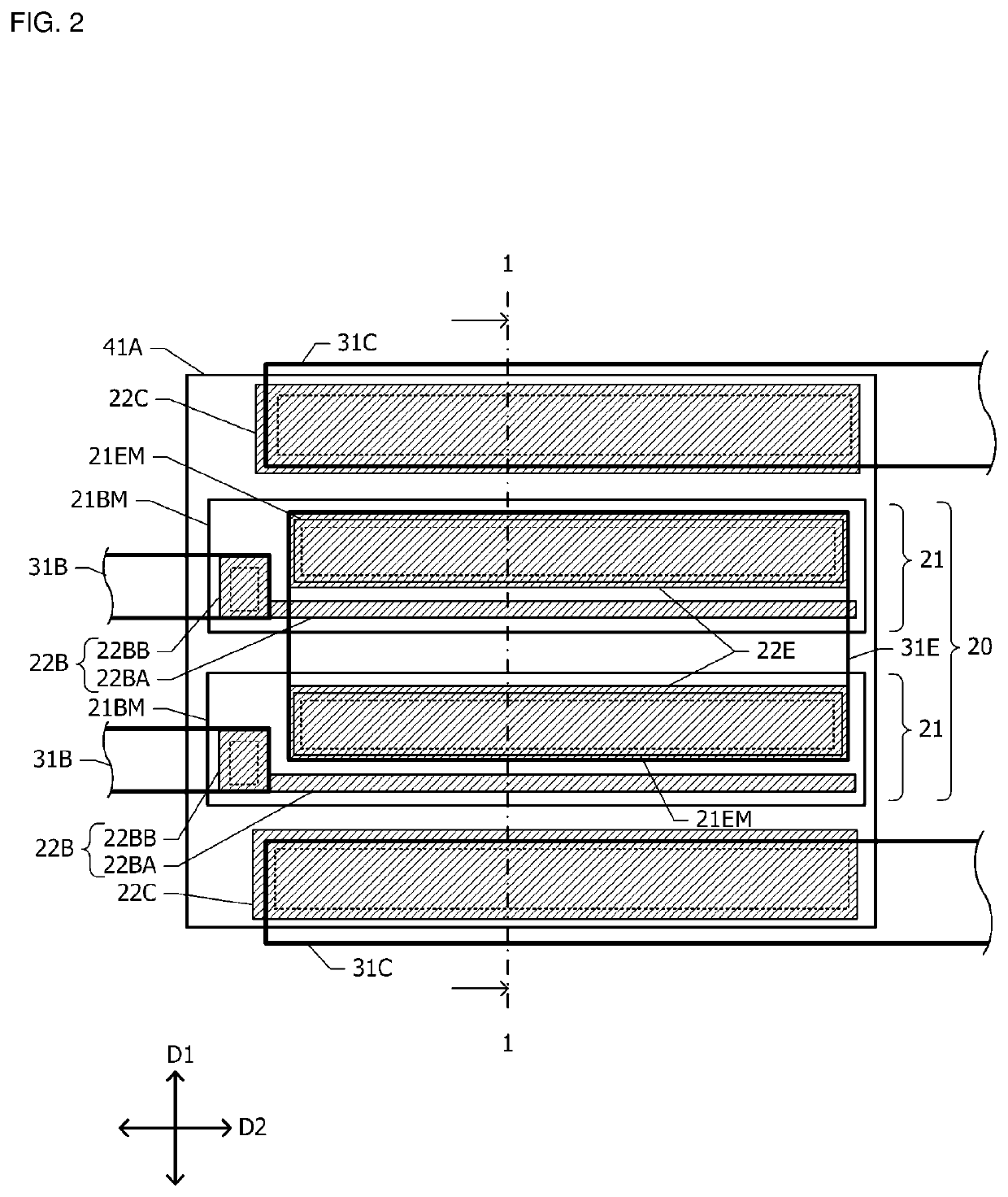
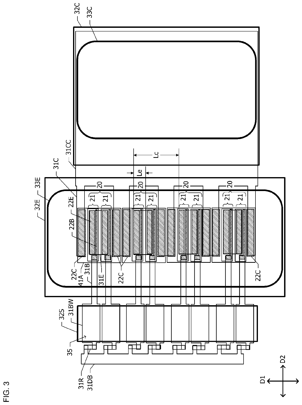
[0031]Referring to FIG. 1 to FIG. 4, a semiconductor device according to the first working example is described. FIG. 1 is a cross-sectional view of a single transistor cell 20 of a semiconductor device according to the first working example. A semiconductor layer is epitaxially grown on a substrate 40 composed of a semiconductor. Part of this semiconductor layer forms a sub-collector layer 41A having n-type conductivity, and the remaining part of this semiconductor layer forms a device isolation region 41B insulated by implanting impurity. Two base mesas 21BM are arranged on the sub-collector layer 41A. The base mesa 21BM includes a collector layer 21C composed of a n-type semiconductor, a base layer 21B composed of a p-type semiconductor arranged on the collector layer 21C, and an emitter layer 21E composed of a n-type semiconductor arranged on the base layer 21B. The collector layer 21C, the base layer 21B, and the emitter layer 21E form an HBT.
[0032]An emitter mesa 21EM is arran...
second working example
[0081]Next, referring to FIG. 7 and FIG. 8, a semiconductor device according to the second working example is described. Hereinafter, the description regarding the configuration common to the semiconductor device according to the first working example (FIG. 1 to FIG. 4) is omitted.
[0082]FIG. 7 is a diagram illustrating a planar spatial relationship among constituent elements of a semiconductor device according to the second working example. FIG. 8 is a diagram illustrating a planar spatial relationship among constituent elements of a single transistor cell 20 of the semiconductor device according to the second working example. As is the case with FIG. 2 and FIG. 3, also in FIG. 7 and FIG. 8, hatching is applied to the emitter electrode 22E, the base electrode 22B, and the collector electrode 22C.
[0083]In the first working example, each of a plurality of the transistor cells 20 includes two unit transistors 21. In contrast, in the second working example, each of a plurality of the tr...
third working example
[0090]Next , referring to FIG. 10 to FIG. 12D, a semiconductor device according to the third working example is described. Hereinafter, the description regarding the configuration common to the semiconductor device according to the first working example (FIG. 1 to FIG. 4) is omitted.
[0091]FIG. 10 is a diagram illustrating a planar spatial relationship among constituent elements of a single transistor cell 20 of a semiconductor device according to the third working example. FIG. 11 is a cross-sectional view of FIG. 10 along the dashed-dotted line 11-11. As is the case with FIG. 2, also in FIG. 10, hatching is applied to the emitter electrode 22E, the base electrode 22B, and the collector electrode 22C.
[0092]In the first working example, a height difference reaching the top surface of the sub-collector layer 41A is formed between the two base mesas 21BM (FIG. 1) in the single transistor cell 20, and the collector layers 21C of the two unit transistors 21 are separated from each other....
PUM
 Abstract
Description
Claims
Application Information
 - R&D
- Intellectual Property
- Life Sciences
- Materials
- Tech Scout
- Unparalleled Data Quality
- Higher Quality Content
- 60% Fewer Hallucinations
Browse by: Latest US Patents, China's latest patents, Technical Efficacy Thesaurus, Application Domain, Technology Topic, Popular Technical Reports.
© 2025 PatSnap. All rights reserved.Legal|Privacy policy|Modern Slavery Act Transparency Statement|Sitemap|About US| Contact US: help@patsnap.com