Wiring board and method for manufacturing wiring board
a manufacturing method and technology for wiring boards, applied in the direction of dielectric characteristics, conductive pattern formation, non-printed masks, etc., can solve the problems of reducing the design flexibility of antennas, the size of portable terminal devices, and the limited space in which antennas are arranged
- Summary
- Abstract
- Description
- Claims
- Application Information
AI Technical Summary
Benefits of technology
Problems solved by technology
Method used
Image

Examples
first modification
(First Modification)
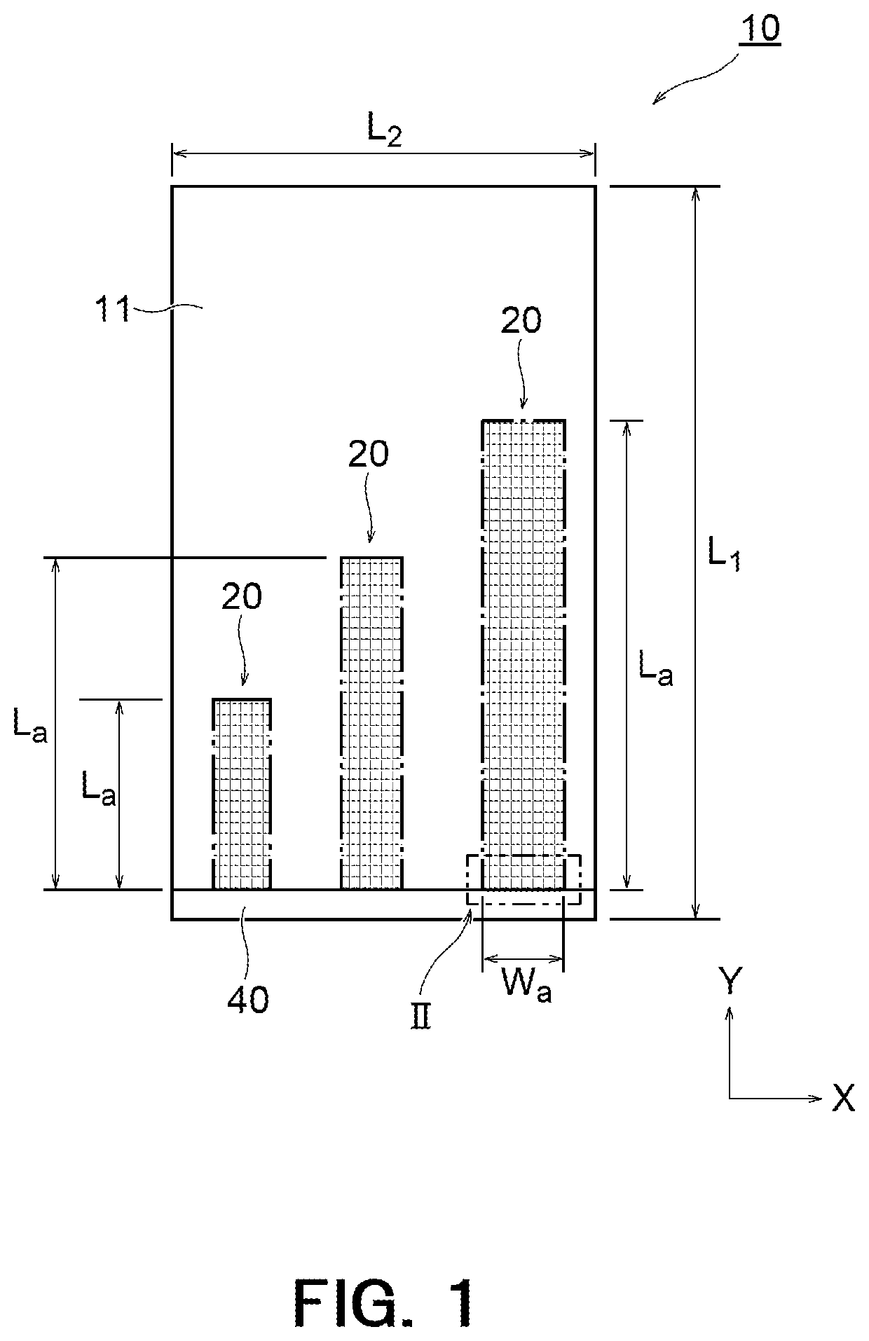
[0098]FIG. 13 illustrates a first modification of the wiring board. The modification illustrated in FIG. 13 differs from the above-described embodiment illustrated in FIGS. 1 to 12 in the structures of the wiring pattern regions 20, and other structures are substantially the same as those of the above-described embodiment. In FIG. 13, portions that are the same as those illustrated in FIGS. 1 to 12 are denoted by the same reference signs, and detailed description thereof is omitted.
[0099]A wiring board 10A illustrated in FIG. 13 includes a substrate 11 and a plurality of wiring pattern regions 20 (20a to 20d) arranged on the substrate 11. Some wiring pattern regions 20 have longitudinal directions different from those of other wiring pattern regions 20. More specifically, some of the wiring pattern regions 20 (20a and 20b) each have a longitudinal direction that is parallel to a side of the substrate 11 (X direction or Y direction). Other wiring pattern regions 2...
second modification
(Second Modification)
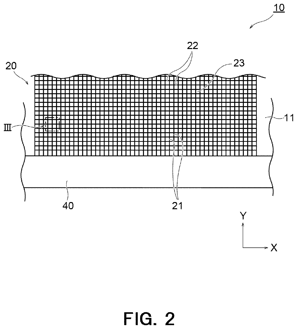
[0101]FIGS. 14A and 14B illustrate a second modification of the present disclosure. FIG. 14A is a sectional view of a first-direction wiring line 21 taken perpendicular to the longitudinal direction thereof, and FIG. 14B is a sectional view of a second-direction wiring line 22 taken perpendicular to the longitudinal direction thereof. The modification illustrated in FIGS. 14A and 14B differs from the above-described embodiment illustrated in FIGS. 1 to 12 in the shapes of the first-direction wiring line 21 and the second-direction wiring line 22, and other structures are substantially the same as those of the above-described embodiment. In FIGS. 14A and 14B, portions that are the same as those in the embodiment illustrated in FIGS. 1 to 12 are denoted by the same reference signs, and detailed description thereof is omitted.
[0102]As illustrated in FIG. 14A, the first-direction wiring line 21 includes a top surface 21a, a bottom surface 21b, and a pair of side sur...
third modification
(Third Modification)
[0118]FIGS. 15A and 15B illustrate a third modification of the present disclosure. FIG. 15A is a sectional view of a first-direction wiring line 21 taken perpendicular to the longitudinal direction thereof, and FIG. 15B is a sectional view of a second-direction wiring line 22 taken perpendicular to the longitudinal direction thereof. The modification illustrated in FIGS. 15A and 15B differs from the above-described second modification illustrated in FIGS. 14A and 14B in cross-sectional shapes of the first-direction wiring line 21 and the second-direction wiring line 22, and other structures are substantially the same as those of the above-described second modification. In FIGS. 15A and 15B, portions that are the same as those in the embodiment illustrated in FIGS. 1 to 14 are denoted by the same reference signs, and detailed description thereof is omitted.
[0119]As illustrated in FIG. 15A, the first-direction wiring line 21 includes a top surface 21a having a proj...
PUM
 Abstract
Description
Claims
Application Information
 - R&D
- Intellectual Property
- Life Sciences
- Materials
- Tech Scout
- Unparalleled Data Quality
- Higher Quality Content
- 60% Fewer Hallucinations
Browse by: Latest US Patents, China's latest patents, Technical Efficacy Thesaurus, Application Domain, Technology Topic, Popular Technical Reports.
© 2025 PatSnap. All rights reserved.Legal|Privacy policy|Modern Slavery Act Transparency Statement|Sitemap|About US| Contact US: help@patsnap.com