High pressure device of resurf containing ferroelectric material and method of making the same

a ferroelectric material and high-pressure technology, applied in the direction of semiconductor devices, electrical apparatus, transistors, etc., can solve the problems of increasing the average on-resistance of the power device, not helping conduct current during on-state, and avalanche breakdown initiated at the surface of the device, so as to reduce the on-resistance (ron) and facilitate integration

Pending Publication Date: 2021-12-23
SIEN QINGDAO INTEGRATED CIRCUITS CO LTD
View PDF3 Cites 0 Cited by
  • Summary
  • Abstract
  • Description
  • Claims
  • Application Information

AI Technical Summary

Benefits of technology

The present invention provides a high voltage semiconductor device comprising a combined junction termination protection structure with a ferroelectric material and a method of making the same to solve problems in conventional junction termination protection structure, such as complex process, large area, high cost, and large on-resistance. The semiconductor power device can raise the breakdown voltage and reduce on-resistance, miniaturize the device size, and it may be easily integrated into a current manufacturing process by simply adding steps of deposition, photolithography, and etching of ferroelectric materials.

Problems solved by technology

Furthermore, it is often the avalanche breakdown is initiated at a surface of device due to a higher local surface electric field than a bulk electric field as related to the interfacial charges.
As the large size of junction termination structure helps the blocking voltage during off-state, it will not help conduct current during on-state but only increasing the average on-resistance of the power device.
Generally, to ensure the breakdown voltage and scaling down the whole device, these junction termination structures may be effectively integrated in the device, but in such a case, process is complex and cost is high.

Method used


Image

  • High pressure device of resurf containing ferroelectric material and method of making the same
  • High pressure device of resurf containing ferroelectric material and method of making the same
  • High pressure device of resurf containing ferroelectric material and method of making the same

Examples


first embodiment

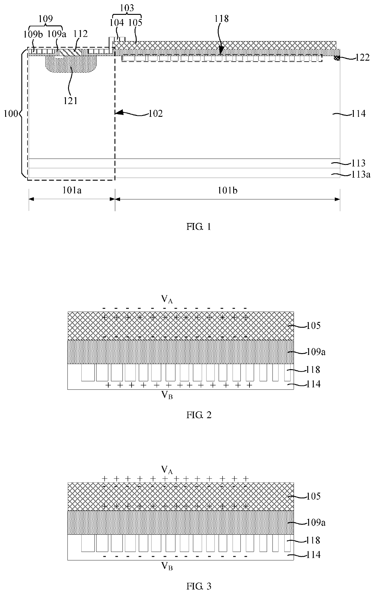
[0073]As shown in FIG. 1, the present embodiment provides a high voltage semiconductor device comprising a combined junction terminal protection structure with a ferroelectric material, and the high voltage semiconductor device comprises:

[0074]an active area 101a formed with the high voltage semiconductor device 102;

[0075]a combined junction terminal protection structure having a RESURF (Reduced Surface Field) structure 103, the RESURF structure 103 comprising a first biasing field plate 104 electrically connecting to the active area 101a and a ferroelectric material layer 105 positioned below the first biasing field plate 104 and in contact with the first biasing field plate 104.

[0076]Please note that the combined junction terminal protection structure has the same function as that of a current high voltage power device, i.e. preventing from early breakdown at a periphery of a main PN junction of the device to increase voltage withstand ability, and meanwhile preventing from an exc...

second embodiment

[0090]The present embodiment provides a method of making a high voltage semiconductor device comprising a combined junction terminal protection structure with a ferroelectric material. With the method, the high voltage semiconductor device comprising the combined junction terminal protection structure with the ferroelectric material of the first embodiment may be made; however, the high voltage semiconductor device of the first embodiment is not limited to the method disclosed in the present embodiment, and therefore, it is readily to be understood that the device of the first embodiment may be made by performing other manufacturing method, i.e. the first embodiment stands for all the implementations with the device structure of the first embodiment. Please refer to the first embodiment for effects of the device structure formed with the manufacturing method of the present embodiment, and they are not repeated here.

[0091]FIGS. 7 and 8 show the method of making the high voltage semic...


PUM

PropertyMeasurementUnit
temperatureaaaaaaaaaa
blocking voltageaaaaaaaaaa
sizeaaaaaaaaaa

Abstract

The present invention provides a high voltage semiconductor device comprising a combined junction terminal protection structure with a ferroelectric material and method of making the same, the device comprises: an active area formed with the high voltage semiconductor device; a combined junction terminal protection structure having a RESURF (Reduced Surface Field) structure, the RESURF structure comprising a first biasing field plate electrically connecting to the active area and a ferroelectric material layer positioned below the first biasing field plate and in contact with the first biasing field plate. The high voltage semiconductor device structure may further assist in raising breakdown voltage (BV) of the device and meanwhile effectively reduce on-resistance (Ron) of the device compared with current junction terminal protection structure, and then miniaturization of the device structure may be fulfilled more easily. Further, the process may be performed easily because only common deposition and patterning processes of Hf-oxide ferroelectric layer should be added to current process.

Description

FIELD OF THE INVENTION[0001]The present invention relates to the technology field of high voltage semiconductor devices, and especially relates to a high voltage semiconductor device comprising a combined junction terminal protection structure with a ferroelectric material and a method of making the same.BACKGROUND OF THE INVENTION[0002]The ability to withstand high voltage of PN junctions of periphery cells dominates the ability to block high voltage across the power semiconductor devices. Currently, a shallow planar junction as resulted from the planar technology, has curved columnar junction along edge and a spherical junction on corner, due to diffused ions of a dopant, higher electric field occurs at the edge and corners, so as to initiate early avalanche breakdown in these areas. As such, a blocking (breakdown) voltage of a PN junction would be lowered. Furthermore, it is often the avalanche breakdown is initiated at a surface of device due to a higher local surface electric f...

Claims


Application Information

Patent Timeline
Patent Type & Authority Applications(United States)
IPC IPC(8): H01L29/06H01L29/78H01L29/66H01L29/10
CPCH01L29/063H01L29/1095H01L29/66681H01L29/7816H01L29/7398H01L29/7823H01L29/7811H01L29/404H01L29/66333H01L29/66712H01L29/402H01L29/7395H01L29/0623H01L29/0878H01L29/861H01L29/7813H01L29/66734H01L29/0619H01L29/0649H01L29/1608H01L29/2003H01L29/408H01L29/7397H01L29/43
Inventor CHI, MIN-HWALI, MINCHANG, RICHARD RU-GIN
Owner SIEN QINGDAO INTEGRATED CIRCUITS CO LTD
Why Eureka
Try Eureka