Spark gap structures for detection and protection against electrical overstress events

a gap structure and sparking technology, applied in the direction of emergency protective arrangements for limiting excess voltage/current, instrumentation, and semiconductor/solid-state device details, can solve the problems of eos events that can occur whether or not the device is powered, damage the integrated circuit (ics), and damage the electronic device. , to achieve the effect of suppressing the formation or propagation of cracks

Active Publication Date: 2021-12-23
ANALOG DEVICES INT UNLTD CO
View PDF8 Cites 0 Cited by
  • Summary
  • Abstract
  • Description
  • Claims
  • Application Information

AI Technical Summary

Benefits of technology

This patent describes a device that can detect and protect against electrical overstress. It consists of two conductive structures that can electrically arc to prevent damage from overcurrent events. The device also includes a barrier structure that helps prevent cracks from forming or spreading due to the overcurrent. This can help to protect sensitive components from damage and ensure the proper functioning of electrical equipment.

Problems solved by technology

Such events can cause damage to an electronic device as a result of the electronic device experiencing a current and / or a voltage that is beyond the specified limits of the electronic device.
In addition, EOS events can occur whether or not the device is powered.
Electrical overstress events, such as transient signal events, can damage integrated circuits (ICs) due to overvoltage conditions and high levels of power dissipation in relatively small areas of the ICs, for example.
High power dissipation can increase IC temperature, and can lead to numerous problems, such as gate oxide punch-through, junction damage, metal damage, surface charge accumulation, the like, or any combination thereof.
However, such characterization is difficult, for example, because the duration of some EOS events can be extremely short.

Method used


Image

  • Spark gap structures for detection and protection against electrical overstress events
  • Spark gap structures for detection and protection against electrical overstress events
  • Spark gap structures for detection and protection against electrical overstress events

Examples


example embodiments

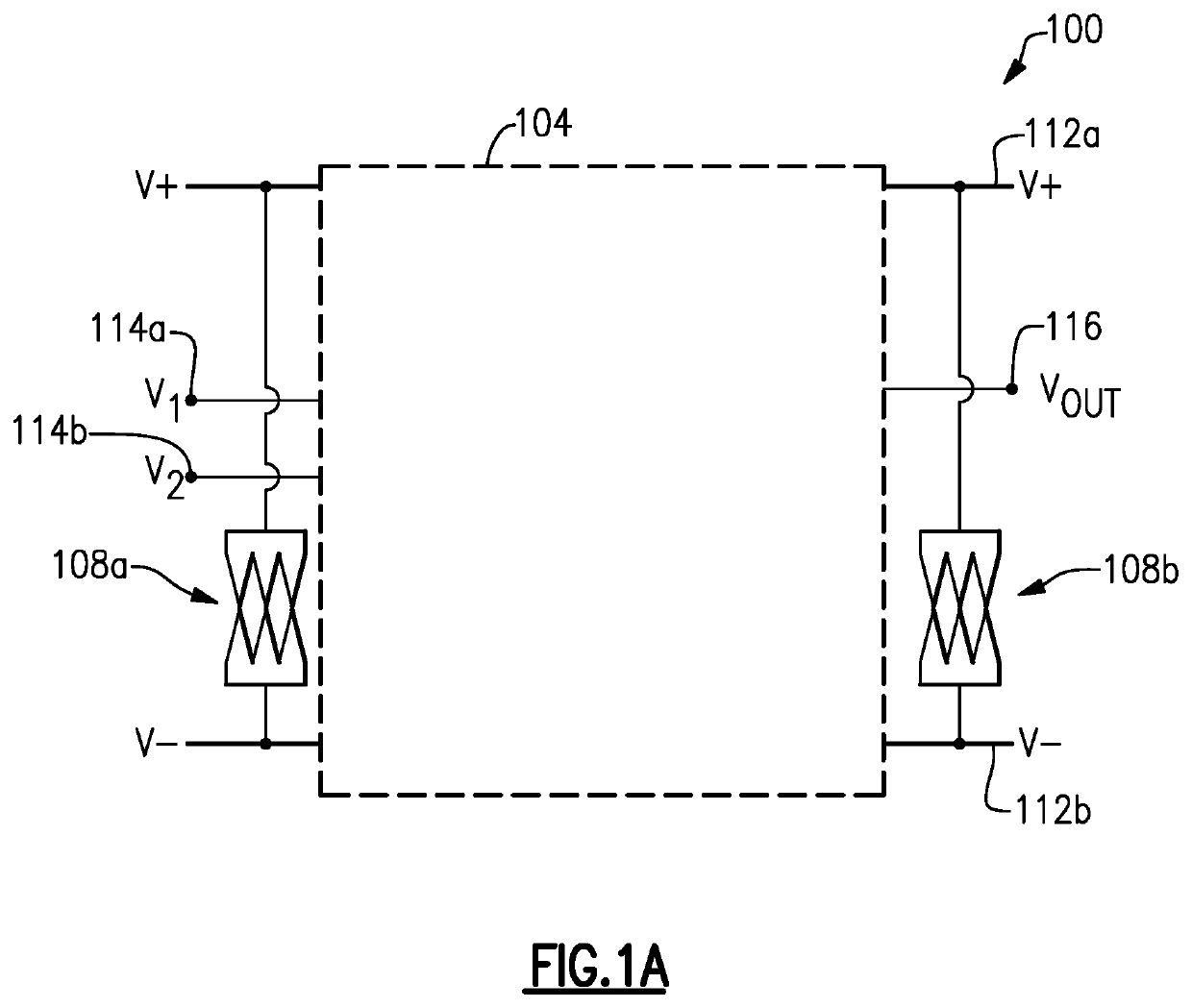
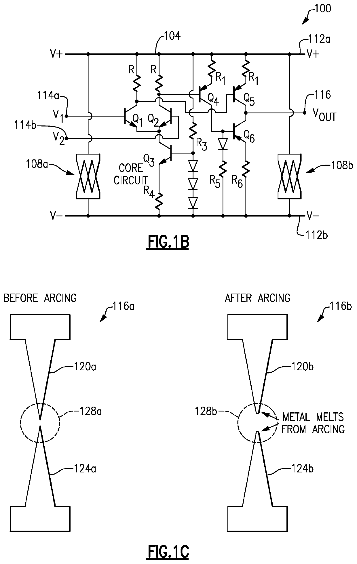
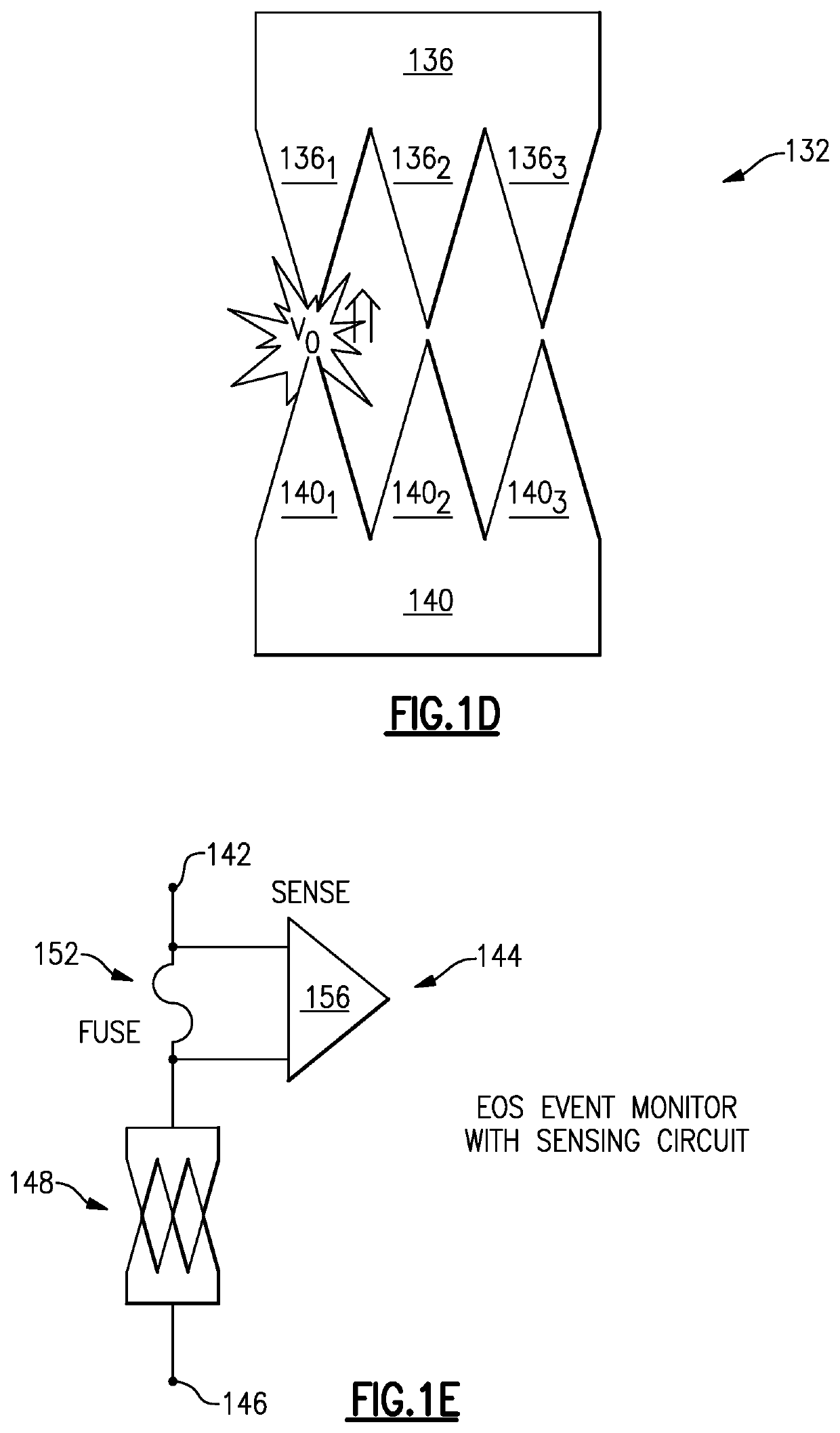
[0429]1. An electrical overstress (EOS) monitor device, comprising:

[0430]an EOS monitor structure comprising a pair of conductive structures configured to electrically arc in response to an EOS event; and

[0431]a sensing circuit configured to detect a change in a physical property of the EOS monitor structure caused by the EOS event.

[0432]2. The EOS monitor device of Embodiment 1, wherein the EOS monitor structure further comprises a resistor connected electrically in series with one of the conductive structures, and wherein the change in the physical property of the EOS monitor structure comprises a change in the resistance of the resistor.

[0433]3. The EOS monitor device of Embodiment 2, wherein the resistor comprises a fuse, and the change in the resistance is caused by an open circuit formed by the fuse in response to the EOS event.

[0434]4. The EOS monitor device of Embodiments 2 or 3, wherein the sensing circuit is electrically connected to the one of the conductive structures, w...


PUM

PropertyMeasurementUnit
electric fieldaaaaaaaaaa
currentaaaaaaaaaa
angleaaaaaaaaaa

Abstract

The disclosed technology generally relates to electrical overstress protection devices, and more particularly to electrical overstress monitoring devices for detecting electrical overstress events in semiconductor devices. In one aspect, an electrical overstress monitor and / or protection device includes a two different conductive structures configured to electrically arc in response to an EOS event and a sensing circuit configured to detect a change in a physical property of the two conductive structures caused by the EOS event. The two conductive structures have facing surfaces that have different shapes;

Description

INCORPORATION BY REFERENCE[0001]This application is a continuation of U.S. patent application Ser. No. 16 / 360,356, now U.S. Pat. No. 11,112,436, filed Mar. 21, 2019, which claims the benefit of priority of U.S. Provisional Application No. 62 / 648,360, filed Mar. 26, 2018, and U.S. Provisional Application No. 62 / 648,745, filed Mar. 27, 2018, the entire disclosures of which are incorporated herein by reference in their entireties for all purposes.[0002]This application is also related to U.S. application Ser. No. 15 / 708,958, filed Sep. 19, 2017, the entire disclosure of which is incorporated by reference herein for all purposes.FIELD OF THE DISCLOSURE[0003]The disclosed technology generally relates to devices for addressing electrical overstress, and more particularly to device for detecting, monitoring, and / or protecting against electrical overstress events in semiconductor devices.BACKGROUND[0004]Certain electronic systems can be exposed to electrical overstress (EOS) events. Such ev...

Claims


Application Information

Patent Timeline
Patent Type & Authority Applications(United States)
IPC IPC(8): G01R19/165G01R31/00G01R31/28H02H9/04H01L27/02H01L23/60H01L23/62H01L23/525H02H9/00
CPCG01R19/16504G01R31/002G01R31/2832G01R31/2856H02H9/00H01L27/0288H01L23/60H01L23/62H01L23/5256H02H9/042G01R31/2879G01R31/2884G01R19/165H02H9/041H02H9/044
Inventor CLARKE, DAVID J.HEFFERNAN, STEPHEN DENISWEI, NIJUNO'DONNELL, ALAN J.MCGUINNESS, PATRICK MARTINBRADLEY, SHAUNCOYNE, EDWARD JOHNAHERNE, DAVIDBOLAND, DAVID M.
Owner ANALOG DEVICES INT UNLTD CO
Why Eureka
Try Eureka