Simultaneous time domain differential sensing and electric field sensing
a technology of differential sensing and electric field, applied in the direction of electronic switching, pulse technique, instruments, etc., can solve problems such as potentially burdensome schemes, and achieve the effect of conserving computing resources
- Summary
- Abstract
- Description
- Claims
- Application Information
AI Technical Summary
Benefits of technology
Problems solved by technology
Method used
Image


Examples
first embodiment
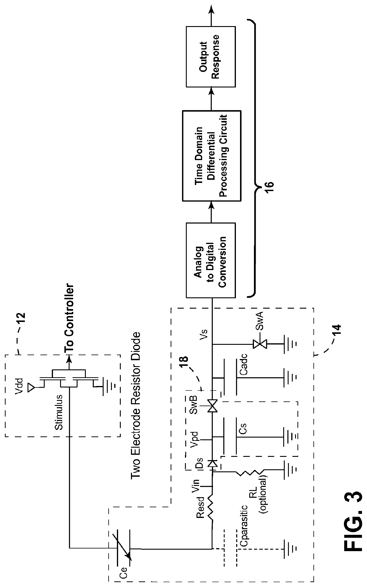
[0064]Referring now to FIG. 3, a circuit diagram for a capacitive sensor in accordance with a first embodiment is illustrated. The capacitive sensor includes a driving circuit 12, a measurement circuit 14, and a signal processing circuit 16. The driving circuit 12 includes a voltage source (Vdd) that is adapted to provide a stimulus voltage, for example the repeating 3V square shown in FIG. 4. The voltage source is optionally controlled by a controller, for example an ASIC, an FPGA, or a microcontroller, which also controls operation of the switches in FIG. 3. The measurement circuit 14 additionally includes a measurement capacitor (Ce), and in particular a strobe electrode capacitively coupled to a sense electrode. The measurement capacitor (Ce) includes a capacitance that changes depending on the presence or absence of touch input on a nearby touch substrate. For example, when “no touch” is present, the measurement capacitor (Ce) may have a lower value of capacitance than when a “...
second embodiment
[0070]Referring to FIG. 7, a circuit diagram for a capacitive sensor in accordance with a second embodiment is illustrated. The capacitive sensor of FIG. 7 is similar in structure and function as the capacitive sensor of FIG. 3, except that the capacitive sensor of FIG. 7 includes a plurality of measurement capacitors (Ce1, Ce2 . . . Ce8) and a corresponding plurality of peak detectors. The peak detectors include a diode (Ds1, Ds2 . . . Ds8), a peak detector capacitor (Cs1, Cs2 . . . Cs8), and a gate switch (SwB1, SwB2 . . . SwB8). The peak detectors are connected through the gate switch (SwB1, SwB2 . . . SwB8) to the sample-and-hold capacitor (Cadc). The measurement circuit 14 can additionally include an electrostatic suppression resistor (Resd1, Resd2 . . . Resd8) and a load resistor (RL1, RL2 . . . RL3) for each measurement capacitor (Ce1, Ce2 . . . Ce8). In this embodiment, the measurement capacitor (Ce1, Ce2 . . . Ce8) includes a single strobe electrode and eight sense electrod...
fourth embodiment
[0073]Referring to FIG. 13, a circuit diagram for a capacitive sensor in accordance with a fourth embodiment is illustrated. The capacitive sensor of FIG. 13 is similar in structure and function as the capacitive sensor of FIG. 9, except that the capacitive sensor of FIG. 13 includes a plurality of measurement capacitors (Ce1, Ce2 . . . Ce8) and a corresponding plurality of peak detectors. Each measurement capacitor (Ce1, Ce2 . . . Ce8) is electrically coupled to a resistor (Rbe1, Rbe2 . . . Rbe8) and a PNP transistor (Q1, Q2 . . . Q8), such that the measurement capacitor (Ce1, Ce2 . . . Ce8) and the resistors (Rbe1, Rbe2 . . . Rbe8) form a delay network across the transistors (Q1, Q2 . . . Q8). Each transistor collector is coupled to a peak detector, and in particular a peak detector diode (Ds1, Ds2 . . . Ds8) and a peak detector capacitor (Cs1, Cs2 . . . Cs8). The peak detector capacitors (Cs1, Cs2 . . . Cs8) are connected through a gate switch (SwB1, SwB2 . . . SwB8) to the sampl...
PUM
 Abstract
Description
Claims
Application Information
 - R&D
- Intellectual Property
- Life Sciences
- Materials
- Tech Scout
- Unparalleled Data Quality
- Higher Quality Content
- 60% Fewer Hallucinations
Browse by: Latest US Patents, China's latest patents, Technical Efficacy Thesaurus, Application Domain, Technology Topic, Popular Technical Reports.
© 2025 PatSnap. All rights reserved.Legal|Privacy policy|Modern Slavery Act Transparency Statement|Sitemap|About US| Contact US: help@patsnap.com