Organic light emitting diode display device and method of manufacturing organic light emitting diode display device

a light-emitting diode and display device technology, which is applied in the direction of organic semiconductor devices, semiconductor devices, electrical devices, etc., can solve the problems of reducing the element may increase, and the driving range of the semiconductor element may be prevented from being shifted, so as to improve the electron mobility of the active layer, improve the photoelectric reliability and channel length scalability of the semiconductor element, and improve the effect of the active layer

Active Publication Date: 2020-11-05
SAMSUNG DISPLAY CO LTD
View PDF0 Cites 0 Cited by
  • Summary
  • Abstract
  • Description
  • Claims
  • Application Information

AI Technical Summary

Benefits of technology

[0027]Since the organic light emitting diode display device herein may include the first gate insulating layer, the active layer may be prevented from being excessively supplied with oxygen. Accordingly, photoelectric reliability and channel length scalability of the semiconductor element may be improved, and a driven range of the semiconductor element may be prevented from being shifted.
[0028]Excess oxygen of the second gate insulating layer may pass through the first gate insulating layer, and the amount of the excess oxygen may be transferred to the active layer during the heat treatment process that may be performed to improve electron mobility of the active layer. Accordingly, the heat treatment process and the oxygen transfer process may be simultaneously performed on the active layer during a single processing stage provided by the heat treatment process. Accordingly, the manufacturing cost of the organic light emitting diode display device may be relatively reduced.
[0029]In a case that the oxygen may be supplied to the active layer, the photoelectric reliability and the channel length scalability of the semiconductor element may be ensured. Thus, even when the semiconductor element including the active layer having a relatively short channel region is small in size, the characteristics and functionality of the semiconductor element may be maintained.

Problems solved by technology

However, in a case that the channel region decreases, dispersion of a threshold voltage of the semiconductor element may increase, and photoelectric reliability and channel length scalability of the semiconductor element may decrease.
However, in a case that the insulating layer directly contacts the active layer, the oxygen may be excessively provided in the channel region, and thus a driven range of the semiconductor element may be shifted.

Method used


Image

  • Organic light emitting diode display device and method of manufacturing organic light emitting diode display device
  • Organic light emitting diode display device and method of manufacturing organic light emitting diode display device
  • Organic light emitting diode display device and method of manufacturing organic light emitting diode display device

Examples


Embodiment Construction

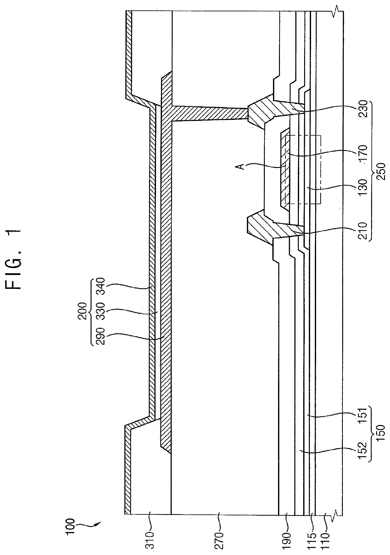
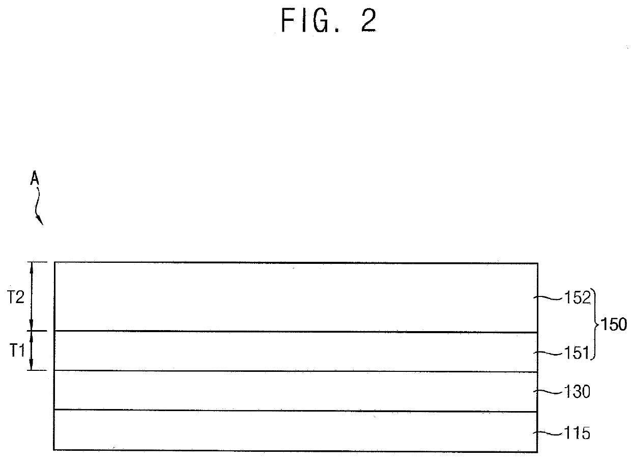
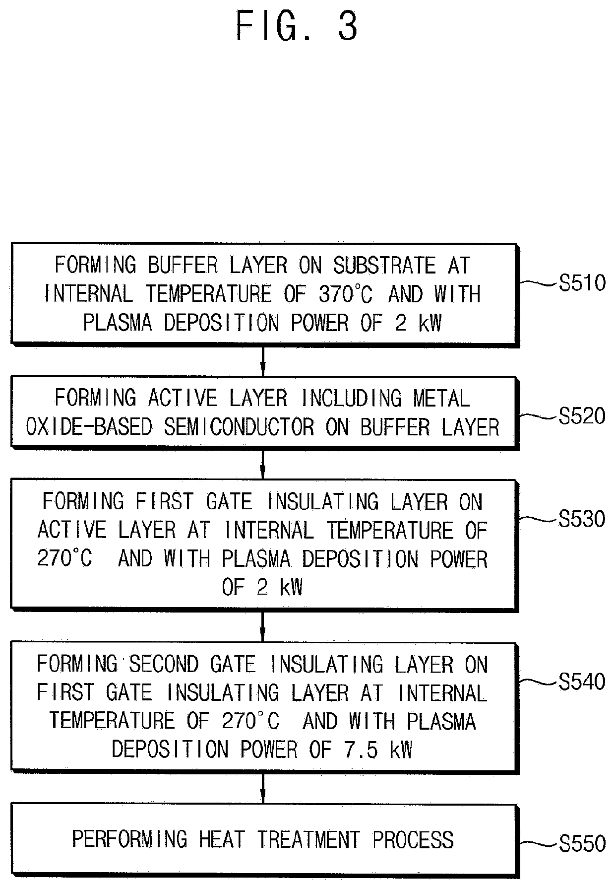
[0041]Hereinafter, an organic light emitting diode display device and a method of manufacturing an organic light emitting diode display device according to embodiments of the disclosure will be described in detail with reference to the accompanying drawings.

[0042]Although aspects of the disclosure may be modified in various manners and have additional embodiments, embodiments are illustrated in the accompanying drawings and will be mainly described in the specification. However, the scope of the disclosure is not limited to the embodiments in the accompanying drawings and the specification and should be construed as including all the changes, equivalents and substitutions included in the spirit and scope of the disclosure. Some of the parts which are not associated with the description may not be provided in order to describe various embodiments and like reference numerals refer to like elements throughout the specification.

[0043]Further, in the specification, the phrase “in a plan ...


PUM

PropertyMeasurementUnit
lengthaaaaaaaaaa
temperatureaaaaaaaaaa

Abstract

An organic light emitting diode display device includes a substrate, an active layer disposed on the substrate and including a metal oxide-based semiconductor, a gate electrode disposed on the active layer, an insulating layer disposed on the gate electrode, source and drain electrodes disposed on the insulating layer, a light emitting element on the source and drain electrodes, and a gate insulating layer between the active layer and the gate electrode. The gate insulating layer includes first and second gate insulating layers. The first gate insulating layer directly contacts the active layer and has a first amount of nitrogen. The second gate insulating layer is disposed on the first gate insulating layer and has a second amount of nitrogen that is different from the first amount of nitrogen.

Description

CROSS-REFERENCE TO RELATED APPLICATION[0001]This application claims priority under 35 USC § 119 to Korean Patent Application No. 10-2019-0052609, filed on May 3, 2019 in the Korean Intellectual Property Office (KIPO), the entire disclosure of which is incorporated herein by reference.BACKGROUND1. Field[0002]Embodiments relate generally to an organic light emitting diode display device and a method of manufacturing organic light emitting diode display device. More particularly, such embodiments relate to an organic light emitting diode display device including a metal oxide-based semiconductor element and a method of manufacturing the organic light emitting diode display device including a metal oxide-based semiconductor element.2. Description of the Related Art[0003]A flat panel display device may be used to replace a cathode ray tube display device because the flat panel display device may have light weight and thin features. A liquid crystal display device and an organic light emi...

Claims


Application Information

Patent Timeline
Patent Type & Authority Applications(United States)
IPC IPC(8): H01L27/32H01L51/56
CPCH01L27/3246H01L2227/323H01L2251/303H01L27/3262H01L51/56H01L27/1225H01L29/4908H01L29/7869H01L29/66969H10K59/1213H01L27/1237H01L27/1214H01L29/78606H01L21/02274H01L21/324H01L29/78618H10K71/00H10K59/122H10K59/1201H10K2102/00
Inventor BANG, SEOKHWANKIM, JONG-INKIM, KANGNAMLEE, WOOGEUNLIM, SUNG-HOONCHAE, SOOJUNG
Owner SAMSUNG DISPLAY CO LTD
Why Eureka
Try Eureka