Conductive coating material and production method for shielded package using conductive coating material
a technology of conductive coating and production method, which is applied in the direction of electrically conductive paint, localised screening, coating, etc., can solve the problems of increased noise generation of electronic parts, and easy erroneous operation of electronic parts, etc., to ensure the conductivity of the coating film, easy formation of shield layer, excellent shielding
Active Publication Date: 2020-09-24
TATSUTA ELECTRICWIRE & CABLE
View PDF0 Cites 0 Cited by
- Summary
- Abstract
- Description
- Claims
- Application Information
AI Technical Summary
Benefits of technology
The conductive coating material described in this patent can create a thin but highly effective shield layer that protects and adheres to a package. It is easy to apply, affordable, and can be produced efficiently using standard equipment. Overall, this material provides an improvement in shielding and protection for electronic packages.
Problems solved by technology
Such electronic parts for wireless communication have a problem in that the electronic parts not only easily generate noises but also are highly sensitive to noises, and, when exposed to noises from outside, the electronic parts are easily caused to carry out erroneous operations.
However, when the mounting density is increased, there occurs a problem in that not only electronic parts as sources for generating noises are increased but also electronic parts affected by the noises are increased.
However, in a case where a shield layer is formed by spray coating using a solution made of metal particles and a solvent, there is a problem in that favorable shielding properties are not obtained and adhesion between the shield layer and a package deteriorates.
However, all of these methods require large-scale equipment and have a problem in that it is easy to entrain bubbles when a conductive resin is filled in a groove portion.
However, the technology has a problem in that the apparatus is expensive, the time required for formation of a shield layer is also long, the cost is high, and it is hard to form a coating film on a side surface of an electronic part.
In addition, in conventional conductive coating materials, other than using pure silver powders, it was difficult to obtain favorable conductivity and shielding properties in a case of a film thickness of 10 μm or less.
However, in a case where the conductive coating material is applied thick, drying of a solvent is slow.
In a portion in which the conductive coating material is thin, conductivity may not be obtained and thus the electromagnetic wave shield effect of the shield layer is not sufficient.
Method used
View moreImage
Smart ImageViewing Examples

Examples
examples
[0076]Hereinafter, the content of the present invention will be described in detail based on examples, but the present invention is not limited to the following. In addition, hereinafter, “part” or “%” is based on mass unless particularly mentioned.
1. Preparation and Evaluation of Conductive Coating Material
Login to View More PUM
| Property | Measurement | Unit |
|---|---|---|
| viscosity | aaaaa | aaaaa |
| viscosity | aaaaa | aaaaa |
| thickness | aaaaa | aaaaa |
Abstract
A conductive coating material is disclosed including at least (A) 100 parts by mass of a binder component including a solid epoxy resin that is a solid at normal temperature and a liquid epoxy resin that is a liquid at normal temperature, (B) 500 to 1800 parts by mass of metal particles that have a tap density of 5.3 to 6.5 g / cm3 with respect to 100 parts by mass of the binder component (A), (C) 0.3 to 40 parts by mass of a curing agent that contains at least one imidazole type curing agent with respect to 100 parts by mass of the binder component (A), and (D) 150 to 600 parts by mass of a solvent with respect to 100 parts by mass of the binder component (A).
Description
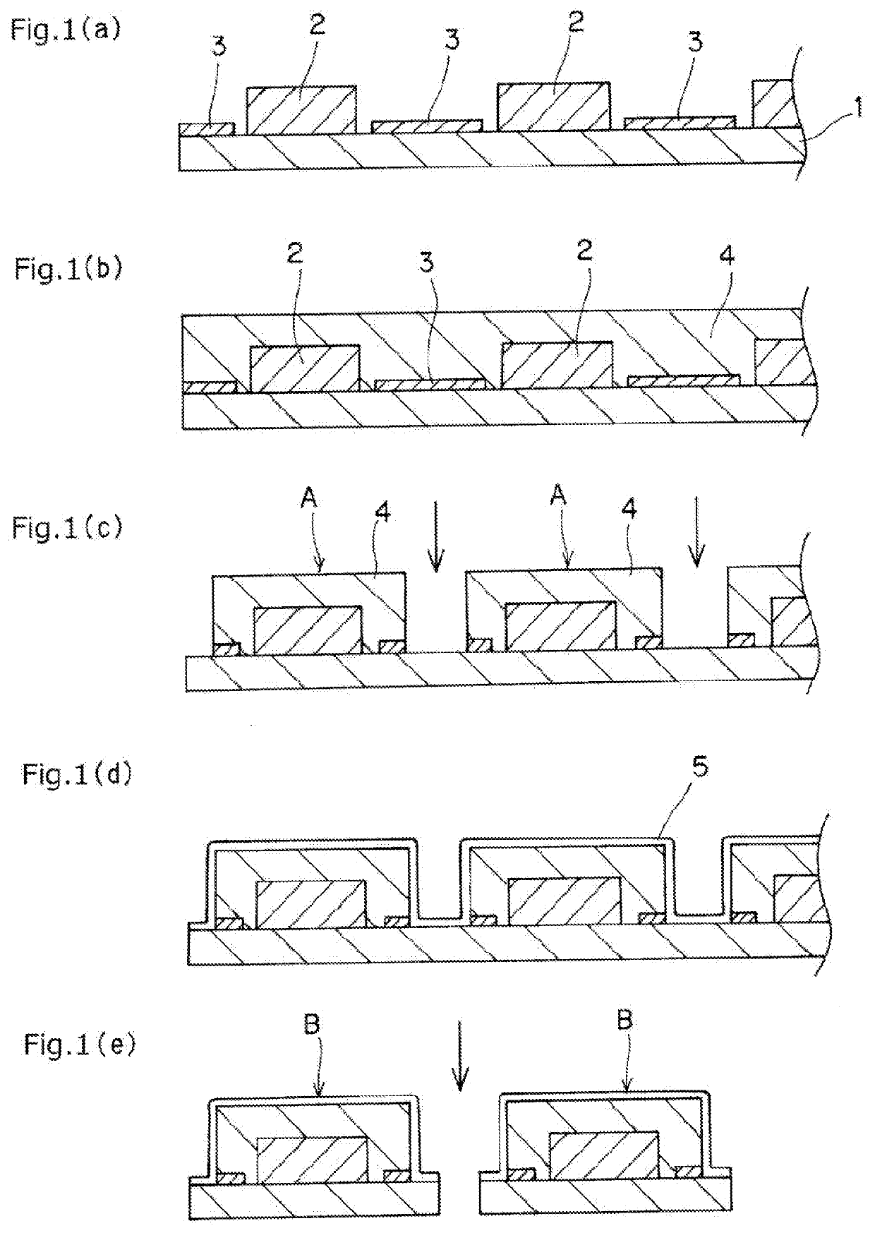
TECHNICAL FIELD[0001]The present invention relates to a conductive coating material and a production method for a shielded package using the conductive coating material.BACKGROUND ART[0002]In recent years, in electronic devices such as portable telephones and tablet terminals, a lot of electronic parts for wireless communication to transmit high-volume data have been mounted. Such electronic parts for wireless communication have a problem in that the electronic parts not only easily generate noises but also are highly sensitive to noises, and, when exposed to noises from outside, the electronic parts are easily caused to carry out erroneous operations.[0003]Meanwhile, in order to obtain miniaturization and weight reduction as well as high functions of electronic devices, it is required to increase mounting density of electronic parts. However, when the mounting density is increased, there occurs a problem in that not only electronic parts as sources for generating noises are increas...
Claims
Login to View More Application Information
Patent Timeline
 Patent Type & Authority Applications(United States)
IPC IPC(8): C09D5/24C09D7/40C09D7/61C09D7/20C09D7/63C09D163/10H05K9/00H01L23/29H01L23/31
CPCH05K9/0081C08K5/13C09D7/61C08K2201/003C09D163/10H01L23/293C08K2201/001C08K2003/085H01L23/31C08K3/08C09D7/20C09D5/24C09D7/63C08K9/02C09D7/70C09D161/04H01B1/22H01L21/561H01L23/3121H01L23/552C08G59/3218C08G59/621C08G59/5073C09D163/04C08K2003/0806C08K2003/0831C08K2003/0862H05K9/0083C08K7/00H05K9/0024C09D163/00H01L23/28C08K5/3445
Inventor UMEDA, HIROAKIMATSUDA, KAZUHIROYUKAWA, KEN
Owner TATSUTA ELECTRICWIRE & CABLE
Features
- R&D
- Intellectual Property
- Life Sciences
- Materials
- Tech Scout
- Unparalleled Data Quality
- Higher Quality Content
- 60% Fewer Hallucinations
Learn More Browse by: Latest US Patents, China's latest patents, Technical Efficacy Thesaurus, Application Domain, Technology Topic, Popular Technical Reports.
© 2025 PatSnap. All rights reserved.Legal|Privacy policy|Modern Slavery Act Transparency Statement|Sitemap|About US| Contact US: help@patsnap.com