Optical module

a technology of optical modules and optical paths, applied in the field of optical modules, can solve the problems of wasting resources, replacing all existing equipment, and large financial costs, and achieve the effects of optimizing the complexity of optical path coupling, reducing the number of optical components, and reducing the cost of operation

Active Publication Date: 2020-08-20
LINKTEL TECH CO LTD
View PDF0 Cites 1 Cited by
  • Summary
  • Abstract
  • Description
  • Claims
  • Application Information

AI Technical Summary

Benefits of technology

[0018]The optical module provided by the invention integrates a large-size signal rate transmission chip, a laser driver chip, a transimpedance limiting amplifier chip, a vertical cavity surface emitting laser chip array and a photodetector chip array in a casing of the QSFP28 package, realizing high-density integrated package requirements for optical modules, and the light-emitting ribbon optical cable and the light-receiving ribbon optical cable are connected with the same interface end MT ferrule, optimizing the complexity of optical path coupling while achieving high-density optical packaging with minimum optical components, and less optical components bring better reliability in optical packaging; and by adopting the optical packaging technology of the invention, the optical path coupling is simple and easy, the coupling efficiency and the coupling yield rate are high, and the utility model is suitable for mass production.

Problems solved by technology

It is impossible to replace all existing equipment at once and it requires a large financial cost and causes a waste of resources.
Upgrading some of the existing systems will introduce a new problem, how new devices can be interconnected with older devices, enabling maximum performance of the data center.
The difficulty of the QSFP28 MLG optical module package lies in the high-density integrated package.
Due to the integration of multiple chips and multi-channel optical components in the QSFP28 package, this poses a high challenge to the packaging technology.

Method used


Image

  • Optical module
  • Optical module
  • Optical module

Examples


first embodiment

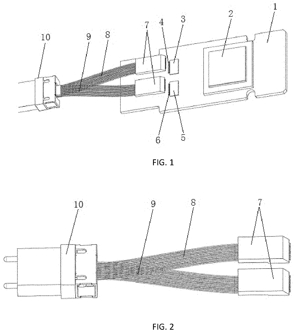
[0028]As shown in FIG. 1, the first embodiment of the present invention provides an optical module. The optical module is a QSFP28 MLG optical module, based on a COB (Chip on Board) process, includes a package (not shown in the figure) and a circuit board 1 located in the package, and further includes an optical component and an electrical interface. The optical port supports 10-channel 10 G light-emitting signals and 10-channel 10 G light-receiving signals. The electrical interface supports 4-channel 25 G electrical signals. The circuit board 1 is provided with a signal rate transmission chip 2, a laser driver chip 3, a transimpedance limiting amplifier chip 5, a vertical cavity surface emitting laser chip array 4, and a photodetector chip array 6.

[0029]The signal rate transmission chip 2 is mounted on the circuit board 1 by SMT. The laser driver chip 3, the transimpedance limiting amplifier chip 5, the vertical cavity surface emitting laser chip array 4, and the photodetector chip...

second embodiment

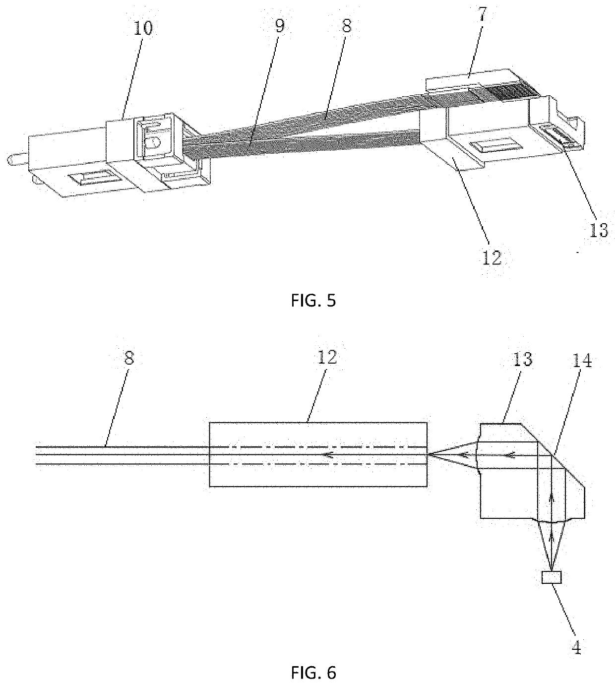
[0037]As shown in FIG. 5, the second embodiment of the present invention provides an optical module, which is different from the optical module provided in the first embodiment of the present invention only in the structure of the optical component, and the other components are identical in structure, and details will not be described herein again.

[0038]In this embodiment, the optical component includes an interface end MT ferrule 10, a light-emitting ribbon optical cable 8 and a light-receiving ribbon optical cable 9 both connected with the interface end MT ferrule 10, a V-groove 7, and a set of combination of intermediate MT ferrule 12 and the lens array 13. The structure of the interface end MT ferrule 10, and its connection manner with the light-emitting ribbon optical cable 8 and the light-receiving ribbon optical cable 9 in the embodiment are the same as those in the first embodiments and will not be described herein again. The light-emitting ribbon optical cable 8 and the lig...


PUM

PropertyMeasurementUnit
conductiveaaaaaaaaaa
reflectionaaaaaaaaaa
densityaaaaaaaaaa

Abstract

The invention provides an optical module including a circuit board, an optical component and an electrical interface, and the circuit board is provided with a signal rate transmission chip, a laser driver chip, a transimpedance limiting amplifier chip, a vertical cavity surface-emitting laser chip array and a photodetector chip array, and the signal rate transmission chip is electrically connected with the laser driver chip and the transimpedance limiting amplifier chip through the first microstrip line, and the optical component includes an interface end MT ferrule, and a light-emitting ribbon optical cable and a light-receiving ribbon optical cable both connected with the interface end MT ferrule, the light-emitting ribbon optical cable is coupled and aligned with the vertical cavity surface-emitting laser chip array, and the light-receiving ribbon optical cable is coupled and aligned with the photodetector chip array, and the electrical interface includes a gold finger disposed on one side of circuit board. The gold finger and the signal rate transmission chip are electrically connected through the second microstrip line. The present invention achieves a high-density optical package while optimizing the complexity of optical path coupling.

Description

CROSS-REFERENCE TO RELATED APPLICATIONS[0001]This application claims priority to International Application No. PCT / CN2018 / 091456, filed on Jun. 15, 2018, which claims the priority benefit of China Patent Application No. 201810293416.5, filed on Mar. 30, 2018. The contents of the above identified applications are incorporated herein by reference in their entirety.FIELD OF THE INVENTION[0002]The present invention relates to the field of optical modules, and in particular, to an optical module.DESCRIPTION OF THE RELATED ART[0003]As big data, cloud computing and cloud storage are growing faster, the bandwidth requirements for processing data traffic in the data center are getting higher and higher, which prompts data center to update and upgrade existing equipment systems in time. Upgrading an existing system is a gradual process. It is impossible to replace all existing equipment at once and it requires a large financial cost and causes a waste of resources. Upgrading some of the exist...

Claims


Application Information

Patent Timeline
Patent Type & Authority Applications(United States)
IPC IPC(8): G02B6/42G02B6/44
CPCG02B6/428G02B6/4403G02B6/425G02B6/4246G02B6/4204G02B6/4251G02B6/4214G02B6/4232G02B6/4257G02B6/4292
Inventor LI, NINGJANG, JIANYANG, XIANWENWU, TIANSHULI, LINKE
Owner LINKTEL TECH CO LTD
Why Eureka
Try Eureka