
Semiconductor device

a technology of semiconductor devices and semiconductors, applied in semiconductor devices, semiconductor/solid-state device details, diodes, etc., can solve the problems of difficult to improve characteristics such as gains, limited number of via-holes, and increase in loss in front-end portions, so as to reduce the resistance of emitters and suppress the effect of output power loss and shorten the distance between via-holes to unit transistors

Active Publication Date: 2020-08-13
MURATA MFG CO LTD
View PDF0 Cites 0 Cited by
  • Summary
  • Abstract
  • Description
  • Claims
  • Application Information

AI Technical Summary

Benefits of technology

The present semiconductor device can reduce emitter resistance without increasing collector resistance and can be used for high-output operation. The input capacitive elements do not affect the arrangement of the via-hole, which allows the distance between the via-hole and the unit transistors to be shortened. This results in a reduction of emitter resistance, preventing a decrease in output power and improving the gain.

Problems solved by technology

In the case where the carrier aggregation is applied to global terminals used in a plurality of countries or regions, a front end including, for example, a power amplifier, a filter, and a switch for radio frequencies of mobile terminals has a complex configuration, resulting in an increase in a loss in a front-end portion.
Therefore, the number of via-holes is limited.
Transistors that are distant from the via-hole have high emitter resistances, and it is difficult to improve characteristics such as gains.

Method used


Image

  • Semiconductor device
  • Semiconductor device
  • Semiconductor device

Examples


first embodiment

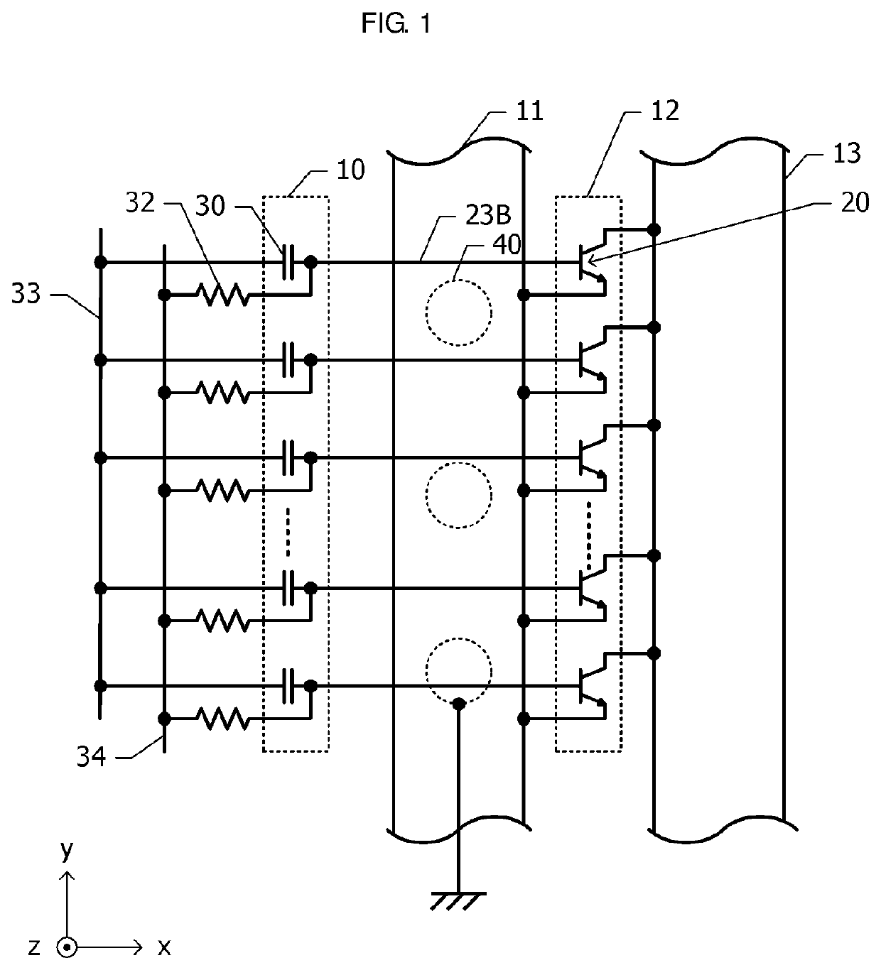
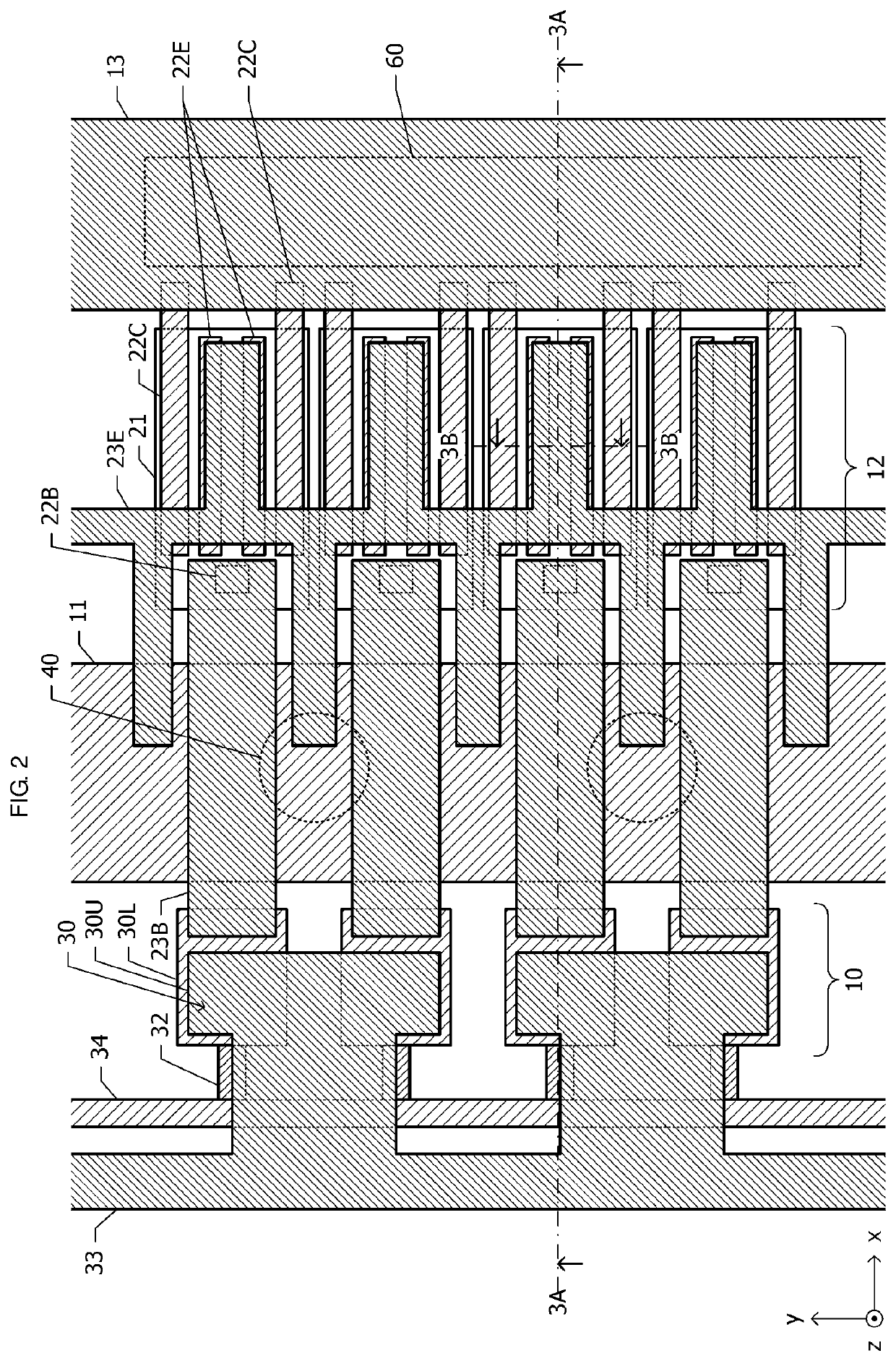
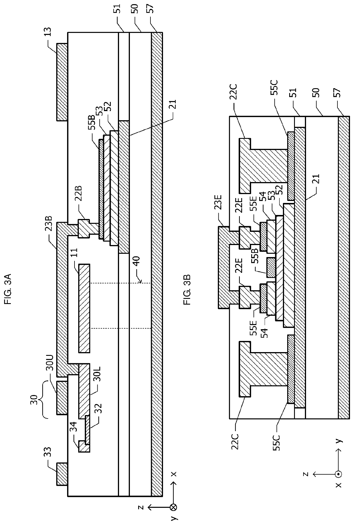
[0020]A semiconductor device according to a first embodiment will be described with reference to FIGS. 1 to 3B. FIG. 1 is a schematic diagram illustrating a planar arrangement of a semiconductor device according to the first embodiment. The semiconductor device according to the first embodiment includes a substrate made of a semiconductor, and a plurality of active elements, a plurality of passive elements, and a plurality of wiring lines are formed on the substrate. An xyz orthogonal coordinate system is defined in which a first surface the substrate is defined as an xy plane and a normal direction of the first surface is defined as a positive direction of a z-axis.

[0021]A plurality of unit transistors 20 each including a base layer, an emitter layer, and a collector layer are arranged on the first surface of the substrate in a y-axis direction. Input capacitive elements 30 are arranged so as to correspond to the plurality of unit transistors 20. The plurality of input capacitive e...

second embodiment

[0059]Next, a semiconductor device according to a second embodiment will be described with reference to FIGS. 4, 5A, and 5B. Hereinafter, descriptions of configurations that are common to those of the semiconductor device according to the first embodiment will be omitted.

[0060]FIG. 4 is a plan view of a semiconductor device according to the second embodiment. FIG. 5A is a sectional view taken along dash-dotted line 5A-5A in FIG. 4, and FIG. 5B is a sectional view taken along dash-dotted line 5B-5B in FIG. 4. In the first embodiment (FIG. 2), the first-layer base wiring line 22B (FIG. 3A) is arranged at an end portion of the base electrode 55B on the side close to the emitter common wiring line 11. In the second embodiment, a first-layer base wiring line 22B (FIGS. 4 and 5A) is arranged at an end portion of a base electrode 55B (FIG. 5A) on the side opposite to an emitter common wiring line 11.

[0061]A second-layer base wiring line 23B (FIG. 5A) passes above the emitter common wiring ...


PUM

PropertyMeasurementUnit
radio frequenciesaaaaaaaaaa
transmission poweraaaaaaaaaa
output poweraaaaaaaaaa

Abstract

A semiconductor device includes a plurality of unit transistors that are arranged on a surface of a substrate in a first direction. Input capacitive elements are arranged so as to correspond to the unit transistors. An emitter common wiring line is connected to emitter layers of the unit transistors. A via-hole extending from the emitter common wiring line to a back surface of the substrate is disposed at a position overlapping the emitter common wiring line. A collector common wiring line is connected to collector layers of the unit transistors. The input capacitive elements, the emitter common wiring line, the unit transistors, and the collector common wiring line are arranged in this order in a second direction. Base wiring lines that connect the input capacitive elements to base layers of the corresponding unit transistors intersect the emitter common wiring line without physical contact.

Description

CROSS-REFERENCE TO RELATED APPLICATION[0001]This application is a Continuation of U.S. patent application Ser. No. 16 / 243,943 filed Jan. 9, 2019, which claims benefit of priority to Japanese Patent Application No. 2018-002030, filed Jan. 10, 2018, the entire content of which is incorporated herein by reference.BACKGROUNDTechnical Field[0002]The present disclosure relates to a semiconductor device.Background Art[0003]With the advance of smartphones, an improvement in the communication speed of mobile communication systems has been desired. A technology called carrier aggregation in which carriers of a plurality of bands are bound together has been introduced as a technology for improving the communication speed. In the case where the carrier aggregation is applied to global terminals used in a plurality of countries or regions, a front end including, for example, a power amplifier, a filter, and a switch for radio frequencies of mobile terminals has a complex configuration, resulting...

Claims


Application Information

Patent Timeline
Patent Type & Authority Applications(United States)
IPC IPC(8): H01L27/06H01L23/522H01L23/528H01L29/66
CPCH01L29/66242H01L23/5223H01L23/528H01L23/5228H01L23/5226H01L27/067H01L27/0647H01L29/732H01L29/0813H01L29/41708H01L29/0692H01L29/66272H01L29/7371
Inventor KOYA, SHIGEKITSUTSUI, TAKAYUKINAKAI, KAZUHITOTANAKA, YUSUKE
Owner MURATA MFG CO LTD
Learn More