
Organic electroluminescent device

a technology of electroluminescent devices and organic el, which is applied in the direction of basic electric elements, semiconductor devices, electrical apparatus, etc., can solve the problems of reducing the light emission area, reducing the lifetime, and high efficiency of organic el devices, so as to improve the electron transport ability, reduce the driving voltage, and reduce the effect of luminous efficiency

Pending Publication Date: 2020-06-18
SOLUS ADVANCED MATERIALS CO LTD
View PDF5 Cites 1 Cited by
  • Summary
  • Abstract
  • Description
  • Claims
  • Application Information

AI Technical Summary

Benefits of technology

The present invention is about an improved electron transporting layer material for organic EL devices that can lower the driving voltage and increase luminous efficiency. This material can also be used in display panels, improving their performance and lifespan.

Problems solved by technology

The demand for larger displays and higher resolutions has led to challenges, for example, high efficiency and long lifespan, for the organic EL devices.
Particularly, the high resolution that may be realized by forming more pixels in the same area results in a decrease in a light emitting area of an organic EL pixel, thus inevitably reducing the lifetime, which has become one of the most important technical problems to be overcome for the organic EL device.
In the fluorescent EL devices which emit light by singlet excitons, the internal quantum efficiency may not theoretically exceed 25% depending on the production ratio, and the external quantum efficiency is regarded to have a limitation of 5%.
As described above, although the phosphorescent EL devices exhibit higher efficiency than fluorescence in terms of luminous efficiency based on the theoretical fact, in the case of blue phosphorescent devices, except green and red, the development level for phosphorescent dopants having deep blue color purity and high efficiency and hosts having a broad energy gap to satisfy such phosphorescent dopants is insufficient, and thus blue phosphorescent devices have not been commercialized yet, and blue fluorescent devices have been used in products.
However, to date, no satisfactory result has been obtained.

Method used


Image

  • Organic electroluminescent device
  • Organic electroluminescent device
  • Organic electroluminescent device

Examples


preparation example

[Preparation Example] Preparation of Compounds ET-01 to ET-21

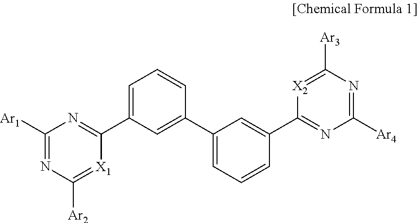
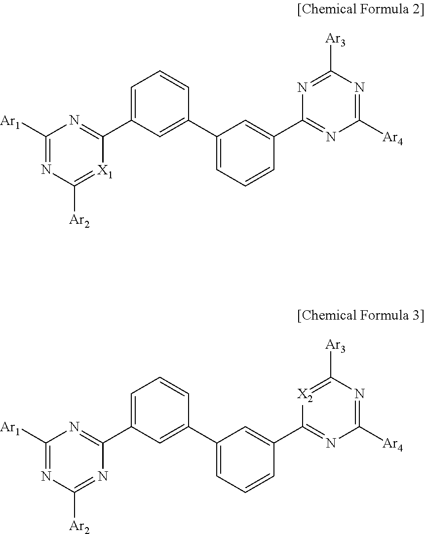
[0138]Compounds represented by the following ET-01 to ET-21 were prepared as the compounds of the present invention, and their LUMO and EHOMO−ELUMO were measured by methods known in the art, respectively, and are shown in Table 1 below.

[0139]For reference, EHOMO−ELUMO was measured using a UV-Vis spectrophotometer (JASCO, V-500), and LUMO was calculated based on EHUMO-ELUMO by measuring HOMO values using an electrochemical measurement equipment (Potentiostat / Galvanostat, Princeton, 273A) in a cyclic voltammetry (CV) method.

[0140]In such a case, Compounds ET-01 to ET-21 are shown below.

TABLE 1CompoundLUMO (eV)EHOMO-ELUMO (eV)ET-012.803.52ET-022.753.50ET-032.763.58ET-042.783.62ET-052.653.48ET-062.683.42ET-072.573.52ET-082.613.47ET-092.633.41ET-102.723.51ET-112.733.48ET-122.823.38ET-132.793.40ET-142.753.47ET-152.643.52ET-162.663.55ET-172.703.49ET-182.643.57ET-192.713.45ET-202.783.55ET-212.793.50

embodiments 1 to 21

[Embodiments 1 to 21] Manufacturing of Blue Organic EL device

[0141]A glass substrate that had been thin-film-coated with indium tin oxide (ITO) to a thickness of 1500 Å was washed ultrasonically with distilled water. After washing with distilled water was completed, the glass substrate was ultrasonically cleaned with a solvent, such as isopropyl alcohol, acetone and methanol, dried, transferred to a UV OZONE cleaner (Power sonic 405, Hwasin Tech) cleaned for 5 minutes using UV, and then transferred to a vacuum evaporator.

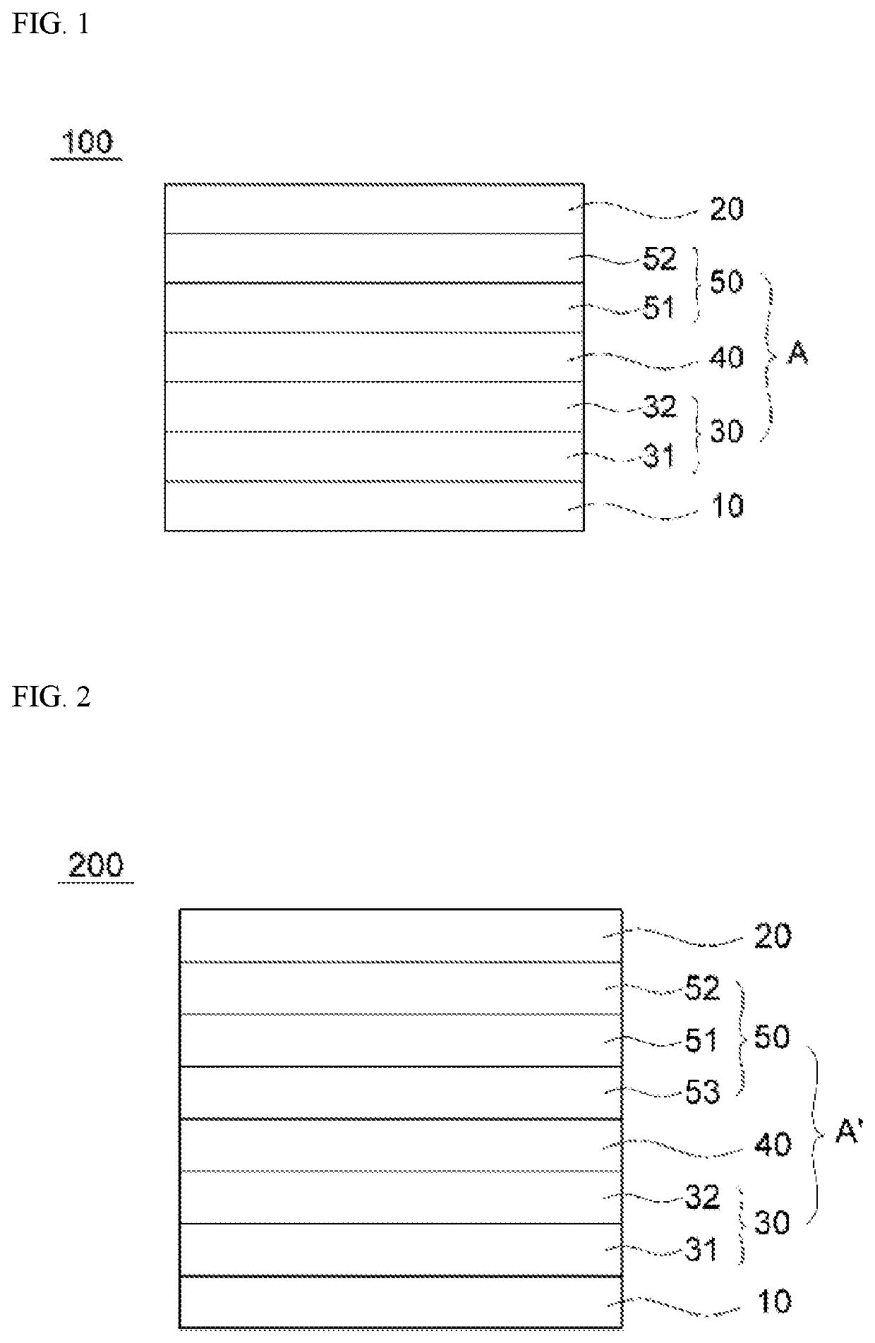
[0142]On the ITO transparent electrode prepared as above, DS-205 (80 nm) / NPB (15 nm) / ADN+5% DS-405 (30 nm) / respective Compounds of Table 1 (30 nm) / LiF (1 nm) / A1 (200 nm) were stack in the order, so that organic EL devices were manufactured.

TABLE 2CompoundThickness (nm)Hole injection layerDS-20580Hole transporting layerNPB15Emissive layerADN + 5% DS-40530Electron transportingET-01~ET-2130layerElectron injection layerLiF1CathodeAl200

experimental example 1

[0147]For each of the blue organic EL devices manufactured in Embodiments 1 to 21 and Comparative Examples 1 to 3, a driving voltage, a current efficiency and a light emission peak at a current density of 10 mA / cm2 were measured and the results are shown in Table 3 below.

TABLE 3ElectronDriving EL Current transportingvoltagepeak efficiencySamplelayer(V)(nm)(cd / A)Embodiment 1ET-013.84548.0Embodiment 2ET-023.54568.9Embodiment 3ET-033.84557.5Embodiment 4ET-044.14537.9Embodiment 5ET-054.04577.2Embodiment 6ET-063.94538.1Embodiment 7ET-073.74557.4Embodiment 8ET-084.04577.6Embodiment 9ET-093.74536.9Embodiment 10ET-103.84557.2Embodiment 11ET-114.14537.5Embodiment 12ET-124.04537.7Embodiment 13ET-134.14577.1Embodiment 14ET-143.84558.1Embodiment 15ET-153.74587.9Embodiment 16ET-163.94577.8Embodiment 17ET-173.74548.2Embodiment 18ET-183.94537.9Embodiment 19ET-193.84527.2Embodiment 20ET-204.04557.8Embodiment 21ET-213.94558.0ComparativeAlq35.44585.5example 1ComparativeT-14.54595.9example 2Comparativ...


PUM

PropertyMeasurementUnit
LUMOaaaaaaaaaa
energy differenceaaaaaaaaaa
ionization potentialaaaaaaaaaa

Abstract

The present invention may provide an organic electroluminescent device which exhibits low driving voltage as well as high efficiency by including an electron transporting layer material having an improved electron transporting ability.

Description

TECHNICAL FIELD[0001]The present invention relates to an organic electroluminescent device capable of achieving both low driving voltage and high efficiency by including an electron transporting layer material that has an improved electron transporting ability.DISCUSSION OF RELATED ART[0002]In 1965, studies on organic electroluminescent devices (hereinafter, “organic EL devices”) led to blue electroluminescence which uses anthracene monocrystals, and in 1987, Tang suggested an organic EL device in a two-layered stack structure which includes a hole layer (NPB) and an emissive layer (Alq3). Afterwards, in order to realize high efficiency and long life characteristics required for commercialization of organic EL devices, a multilayer stack structure that includes, for example, organic layers responsible for hole injection and transporting, organic layers responsible for electron injection and transporting, and an organic layer responsible for inducing combination of the holes and elec...

Claims


Application Information

Patent Timeline
Patent Type & Authority Applications(United States)
IPC IPC(8): H01L51/50H01L51/52H01L51/00
CPCH01L51/5072H01L51/5206H01L51/0067H01L51/5016H01L51/5056H01L51/5004H01L51/5221H01L51/5092H10K85/615H10K85/631H10K85/636H10K85/654H10K85/6576H10K85/6572H10K85/6574H10K50/166H10K50/16H10K85/656H10K50/11H10K2101/40H10K50/171
Inventor HAN, SONG IEEUM, MIN SIKSIM, JAE YILEE, YONG HWANPARK, WOO JAEKIM, TAE HYUNG
Owner SOLUS ADVANCED MATERIALS CO LTD
Learn More