Substrate with an electrically conductive film, substrate with a multilayer reflective film, reflective mask blank, reflective mask and method of manufacturing semiconductor device
- Summary
- Abstract
- Description
- Claims
- Application Information
AI Technical Summary
Benefits of technology
Problems solved by technology
Method used
Image

Examples
Embodiment Construction
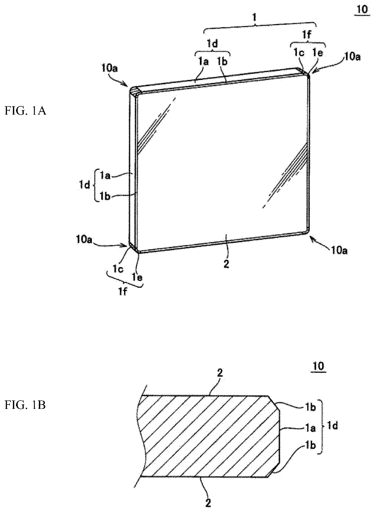
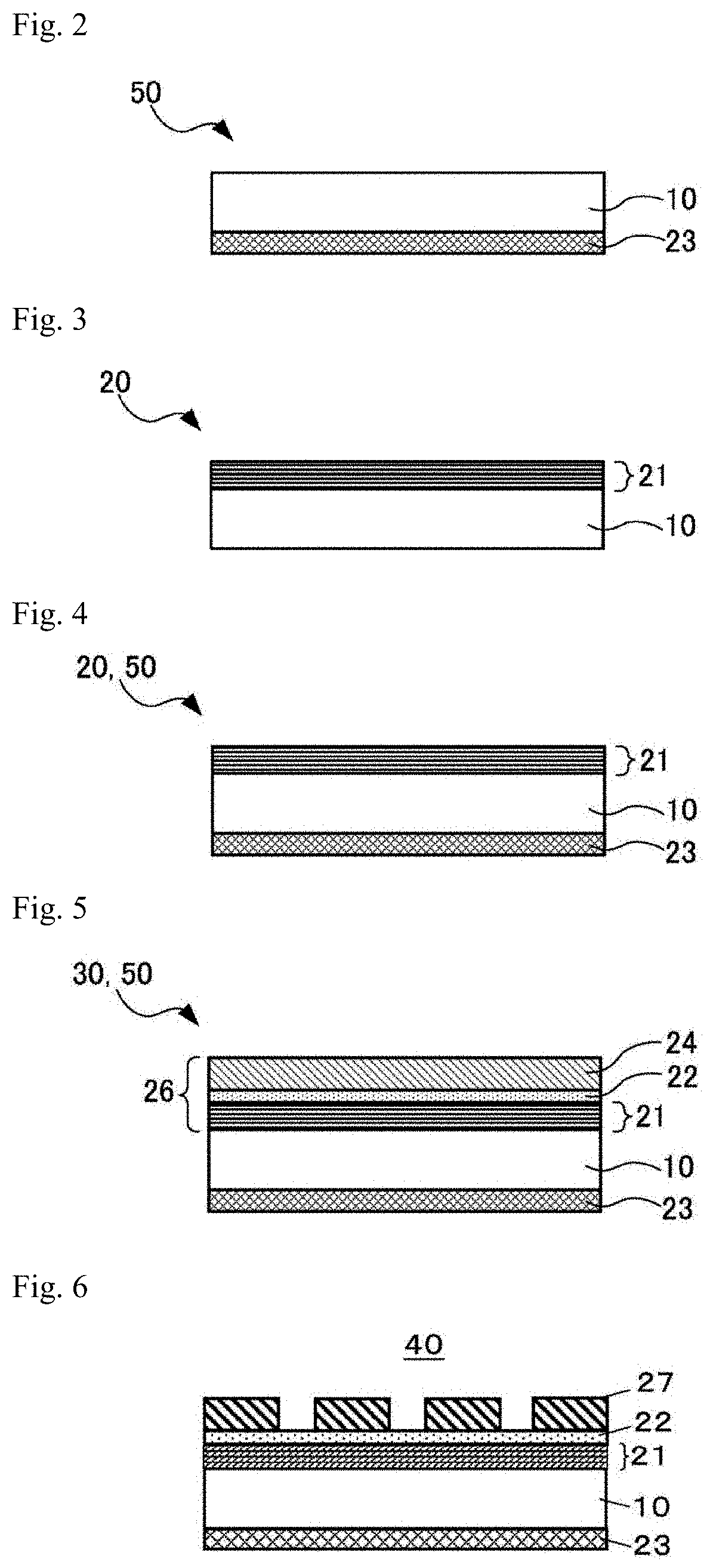
[0186]The following provides an explanation of examples of fabricating the substrate with an electrically conductive film 50, the substrate with a multilayer reflective film 20, the reflective mask blank 30 and the reflective mask 40 of the present disclosure.
[0187]50 of Examples 1 to 5 and Comparative Example 1>
[0188]First, the multilayer reflective film 21 was deposited on the surface of the mask blank substrate 10 for EUV exposure in the manner described below to fabricate substrates with an electrically conductive film 50 of Examples 1 to 5 and Comparative Example 1.
[0189]10>
[0190]Mask blank substrates 10 used to fabricate the substrates for an electrically conductive film of Examples 1 to 5 and Comparative Example 1 were fabricated in the manner described below.
[0191]An SiO2—TiO2-based glass substrate having a size of 152 mm×152 mm and a thickness of 6.35 mm was prepared for use as the mask blank substrate 10, and the front and back surfaces of the glass substrate were sequenti...
PUM
 Abstract
Description
Claims
Application Information
 - R&D Engineer
- R&D Manager
- IP Professional
- Industry Leading Data Capabilities
- Powerful AI technology
- Patent DNA Extraction
Browse by: Latest US Patents, China's latest patents, Technical Efficacy Thesaurus, Application Domain, Technology Topic.
© 2024 PatSnap. All rights reserved.Legal|Privacy policy|Modern Slavery Act Transparency Statement|Sitemap