Silicene electronic device

a technology of electronic devices and silicon, applied in the direction of semiconductor devices, electrical apparatus, transistors, etc., can solve the problems of difficult ohmic contact, achieve the effect of reducing the implantation method, simplifying the implantation process, and simplifying the process

Active Publication Date: 2020-04-30
SAMSUNG ELECTRONICS CO LTD
View PDF2 Cites 2 Cited by
  • Summary
  • Abstract
  • Description
  • Claims
  • Application Information

AI Technical Summary

Benefits of technology

[0031]The silicene electronic device according to the present disclosure may provide a new method for forming an ohmic contact of an electrode. For example, a new method of forming an ohmic contact on a source and a drain of a field effect transistor (FET) of a nanometer level may be provided.
[0032]The s

Problems solved by technology

Furthermore, graphene may not use a silicon process of the related art, but since silicene includes silicon, an existing silicon process may be used for manufacturing a silicene electronic device.
However,

Method used


Image

  • Silicene electronic device
  • Silicene electronic device
  • Silicene electronic device

Examples


Embodiment Construction

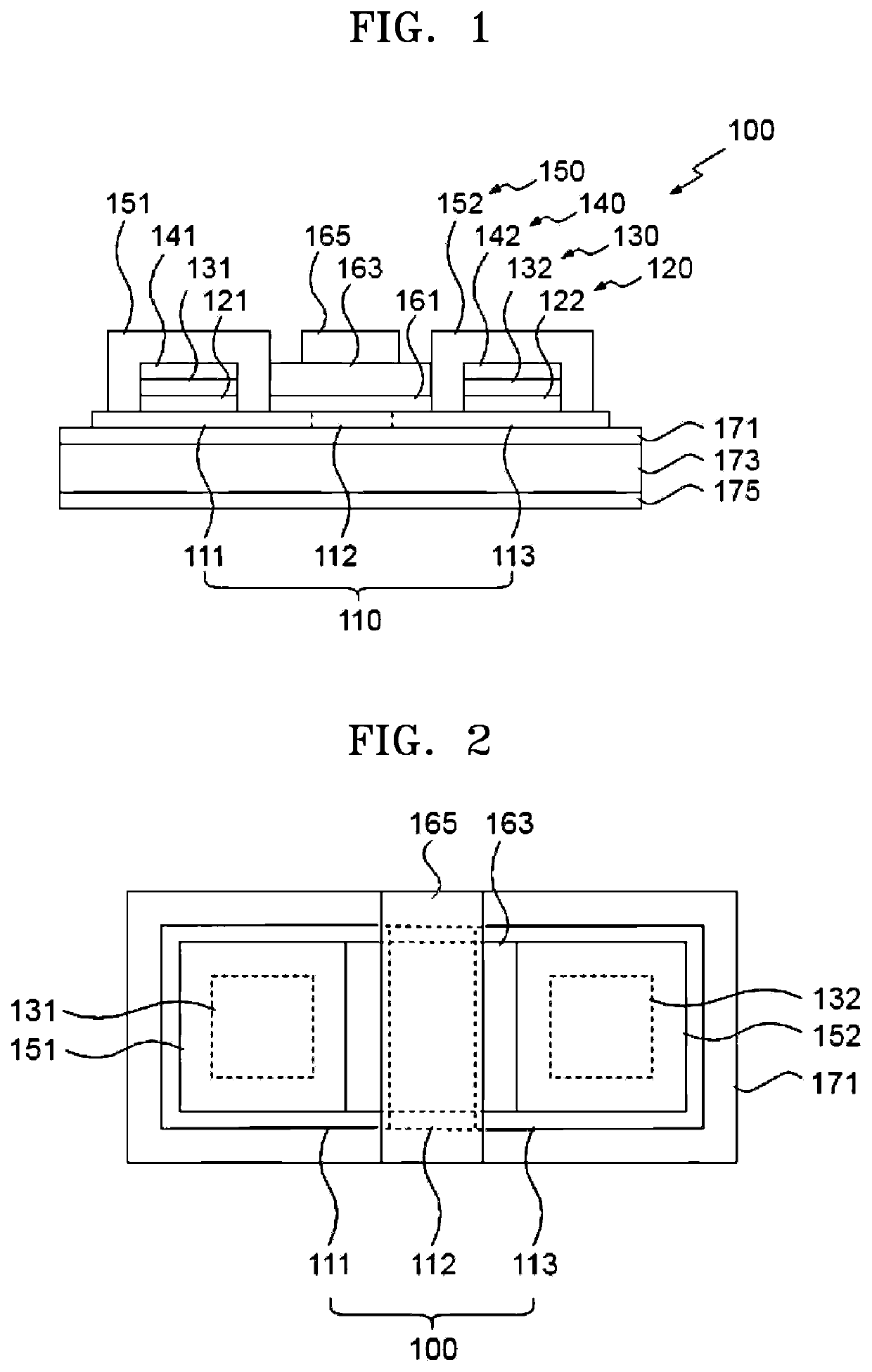
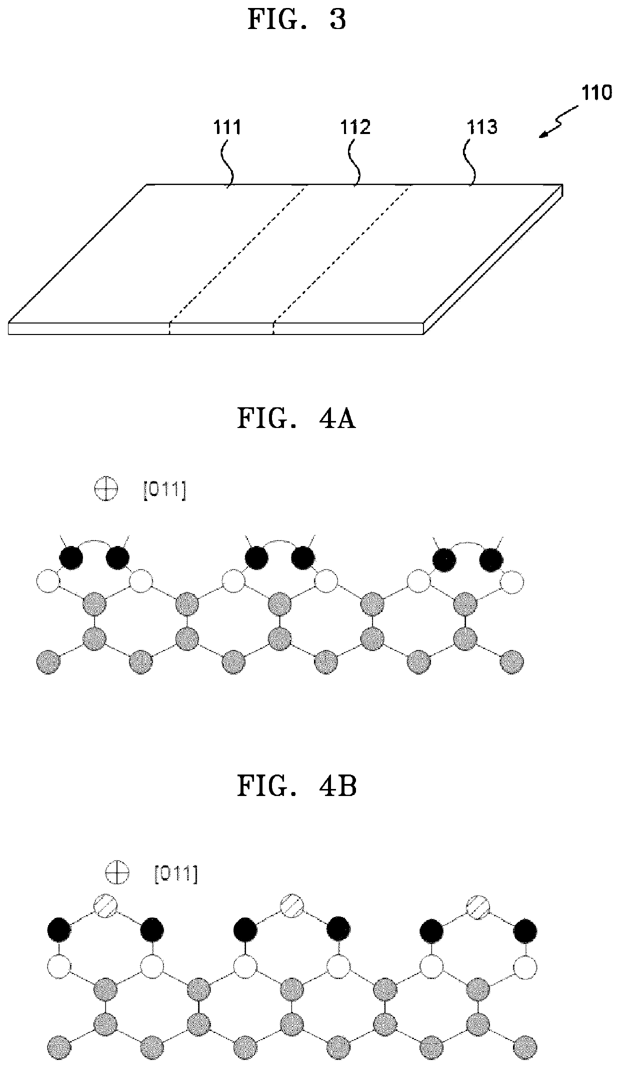
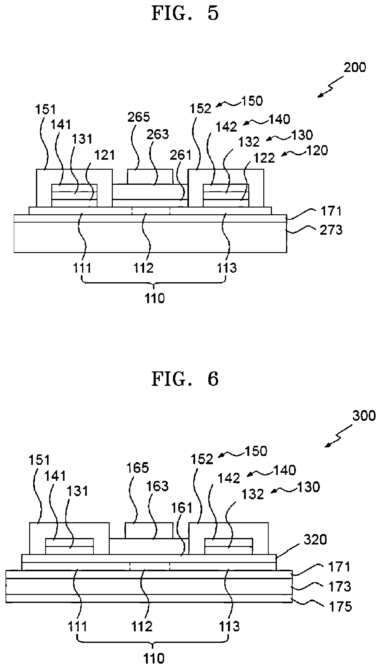
[0048]Reference will now be made in detail to embodiments, examples of which are illustrated in the accompanying drawings. The embodiments may, however, be embodied in many different forms and should not construed as limited to the embodiments set forth herein. Rather, these embodiments are provided so that this disclosure will be thorough and complete, and will fully convey the scope of the invention to those of ordinary skill in the art. The embodiments will be defined by the appended claims. In the entire specification, like reference numerals refer to like elements throughout and, in the drawings, sizes and thicknesses of constituent elements are exaggerated for clarity of explanation.

[0049]Terminology used in the specification will be briefly described and the embodiments will be described in detail.

[0050]Terminology used herein are selected as commonly used by those of ordinary skill in the art in consideration of functions of the embodiments, but may vary according to the tec...


PUM


Abstract

A silicene electronic device includes a silicene material layer. The silicene material layer of the silicene electronic device has a 2D honeycomb structure of silicon atoms, is doped with at least one material of Group I, Group II, Group XVI, and Group XVII, and includes at least one of a p-type dopant region doped with a p-type dopant and an n-type dopant region doped with an n-type dopant. An electrode material layer including a material having a work function lower than the electron affinity of silicene is formed on the silicene material layer.

Description

CROSS-REFERENCE TO RELATED APPLICATION[0001]This application claims the benefit of Korean Patent Application No. 10-2018-0128534, filed on Oct. 25, 2018, in the Korean Intellectual Property Office, the disclosure of which is incorporated herein in its entirety by reference.BACKGROUND1. Field[0002]The present disclosure relates to silicene electronic devices including a silicene material layer.2. Description of the Related Art[0003]Silicene is a material in which silicon atoms as an allotrope form a two-dimensional (2D) honey comb structure like graphene. Since silicene has the same structure as graphene, silicene has a similar band structure to graphene and electron transport is determined by the Dirac equation. Silicene is expected to have a mobility of approximately as high as 106 cm2 / Vs, and also, an electronic device (hereinafter, a silicene electronic device) including a silicene material layer is expected to solve a physical limitation of Si devices of the related art. Further...

Claims


Application Information

Patent Timeline
IPC IPC(8): H01L29/45H01L29/16H01L29/786
CPCH01L29/45H01L29/78684H01L29/78696H01L29/16H01L29/1606H01L29/0847H01L29/778H01L29/51H01L29/47H01L29/7833H01L21/8238
Inventor OH, YOUNGTEKJUNG, JINWOOKKWON, HYEOKSHINSEO, WONTAEKJEON, LNSU
Owner SAMSUNG ELECTRONICS CO LTD
Why Eureka
Try Eureka