
Pad design for thermal fatigue resistance and interconnect joint reliability

Pending Publication Date: 2020-04-16
INTEL CORP
View PDF8 Cites 1 Cited by
  • Summary
  • Abstract
  • Description
  • Claims
  • Application Information

AI Technical Summary

Benefits of technology

The patent text discusses the problem of CTE mismatches between semiconductor packages and printed circuit boards, which can cause stress and damage to interconnect joints. The limited adherence of solder to conventional interconnect structures can also reduce interconnect joint reliability. The patent proposes an interconnect structure that includes micro features formed in a non-solder mask defined pad to absorb stress caused by CTE mismatches. The technical effect of this invention is to improve the reliability of interconnect joints in packaged systems and printed circuit boards.

Problems solved by technology

Pressures to improve the performance capabilities of these systems have caused the number of semiconductor dies in a semiconductor package to increase over time.
Increasing silicon in a package, however, reduces the package's overall coefficient of thermal expansion (CTE).
However, increasing the amount of metallic materials in a PCB increases the PCB's overall CTE.
The reducing CTEs of semiconductor packages and the increasing CTEs of PCBs is increasing the CTE mismatches between these devices.
CTE mismatches create stress between interconnect joints coupling packages and PCBs.
Such stress can curtail the reliable functioning of a packaged system because the stress may damage the interconnect joints.
Adherence of solder used to form an interconnect joint to the conventional interconnect structure is limited.
This is because the flat surface of the conventional interconnect structure has a limited surface area.
The limited adherence can reduce reliability of the subsequently formed interconnect joint because the joint may be incapable of absorbing stress affecting coupled substrates.
For example, the unabsorbed stress can cause cracks in the interconnect joint, cratering of the interconnect structure, etc.
Such mismatches are due to differing CTEs of materials used to form the interconnect structure, the solder, and the other features.
These CTE mismatches create stress that can affect the interconnect structure, the solder, or the other materials.
Due to the limited adherence described above, the interconnect joint and / or the interconnect structure may be incapable of absorbing the stress caused by CTE mismatches, which can in turn damage the interconnect joint and / or the interconnect structure.
These techniques, however, have some drawbacks.
Similar to the underfill materials, glues can be costly to design and manufacture.
Another drawback of using underfill materials and glues is suboptimal control during semiconductor manufacturing and packaging processes.
Also, use of underfill materials and glues limits solder rework due to costs associated with manipulating previously applied underfill materials or glues on interconnect joints.
Additionally, use of underfill materials and glues adds to the CTE mismatches between substrates, which can reduce interconnect joint reliability.
Consequently, some existing techniques for improving interconnect joint reliability are suboptimal.

Method used


Image

  • Pad design for thermal fatigue resistance and interconnect joint reliability
  • Pad design for thermal fatigue resistance and interconnect joint reliability
  • Pad design for thermal fatigue resistance and interconnect joint reliability

Examples


Embodiment Construction

[0019]In the following description, numerous specific details are set forth, such as specific material and structural regimes, in order to provide a thorough understanding of embodiments of the present disclosure. It will be apparent to one skilled in the art that embodiments of the present disclosure may be practiced without these specific details. In other instances, well-known features, such as single or dual damascene processing, are not described in detail in order to not unnecessarily obscure embodiments of the present disclosure. Furthermore, it is to be understood that the various embodiments shown in the Figures are illustrative representations and are not necessarily drawn to scale. In some cases, various operations will be described as multiple discrete operations, in turn, in a manner that is most helpful in understanding the present disclosure, however, the order of description should not be construed to imply that these operations are necessarily order dependent. In pa...


PUM


Abstract

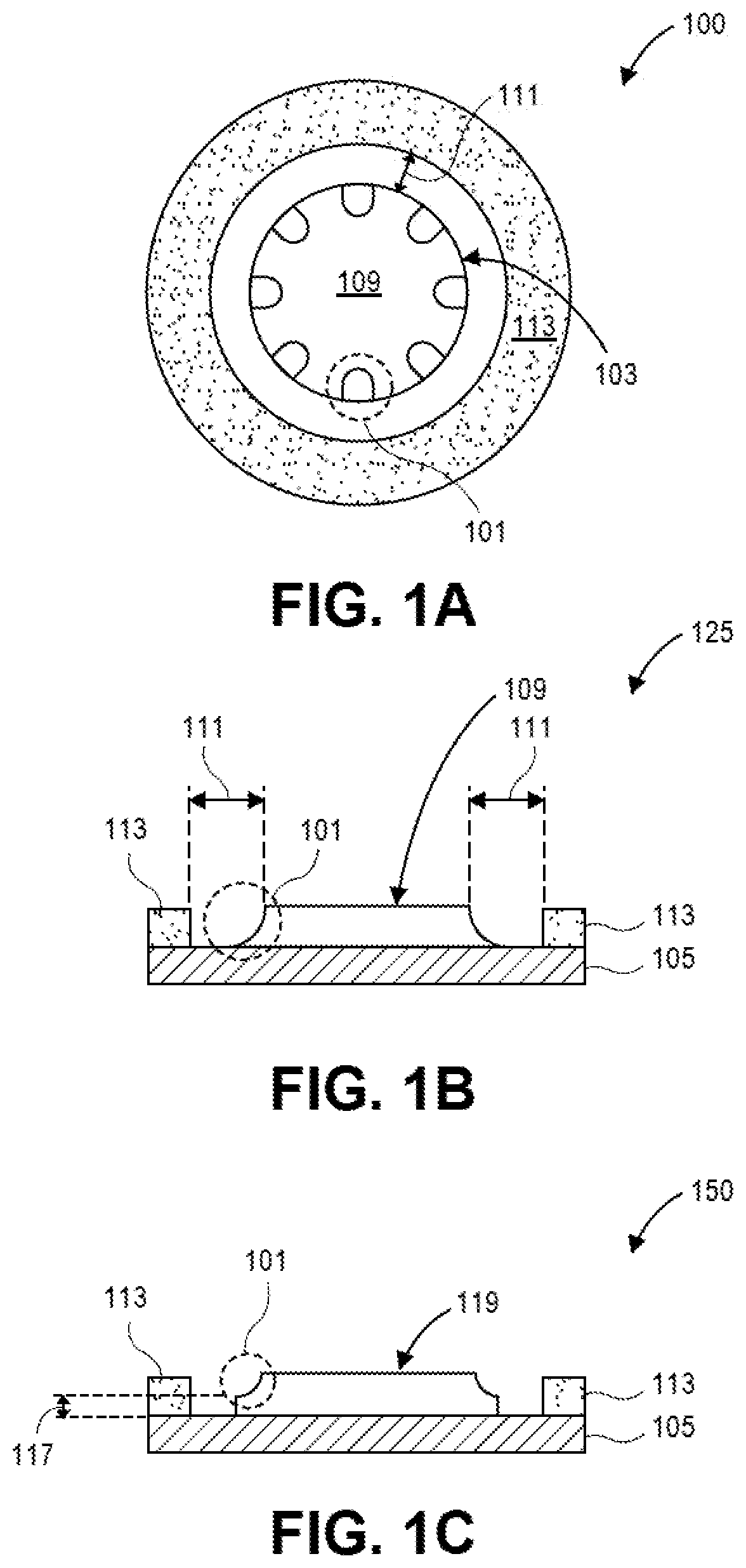
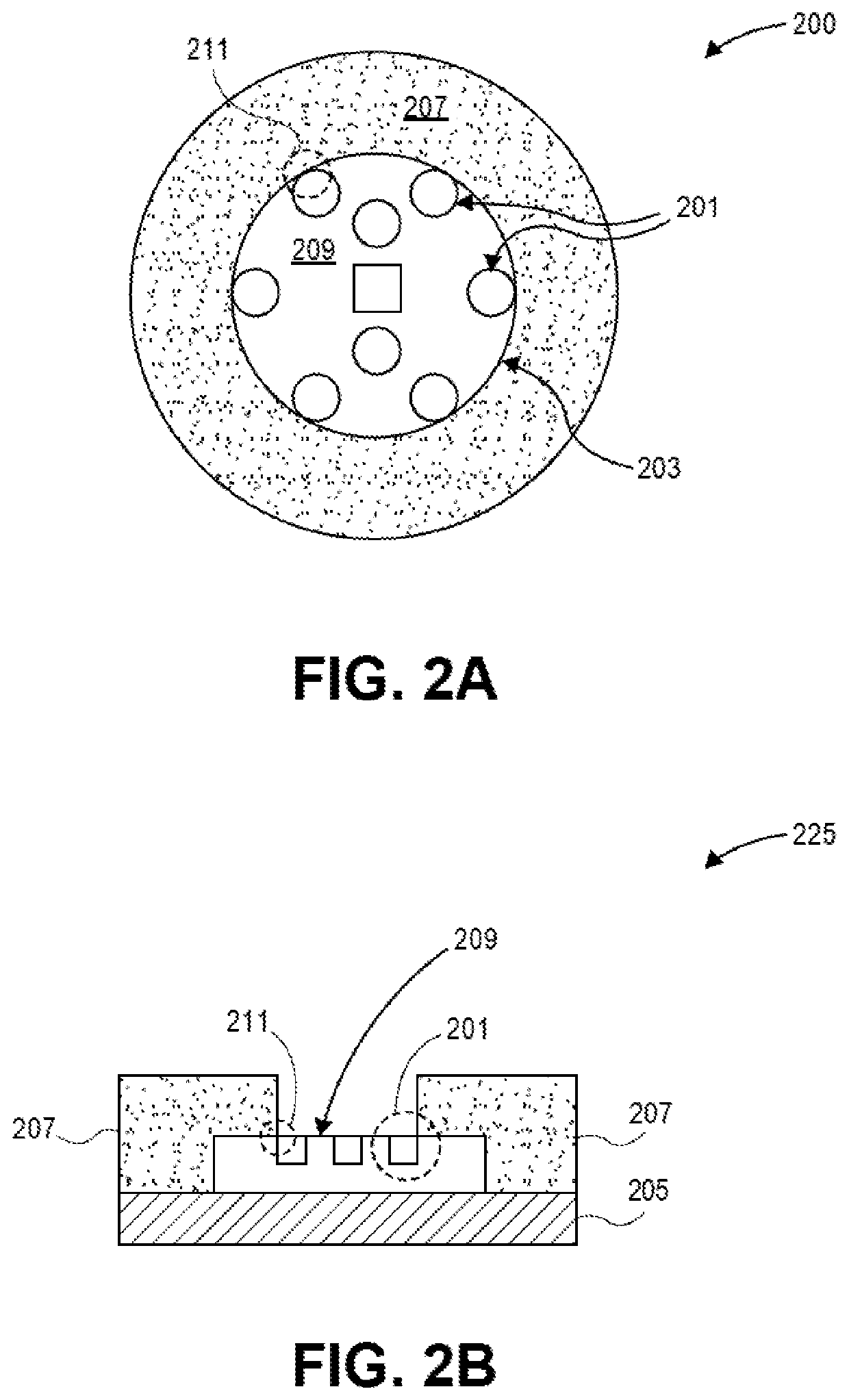
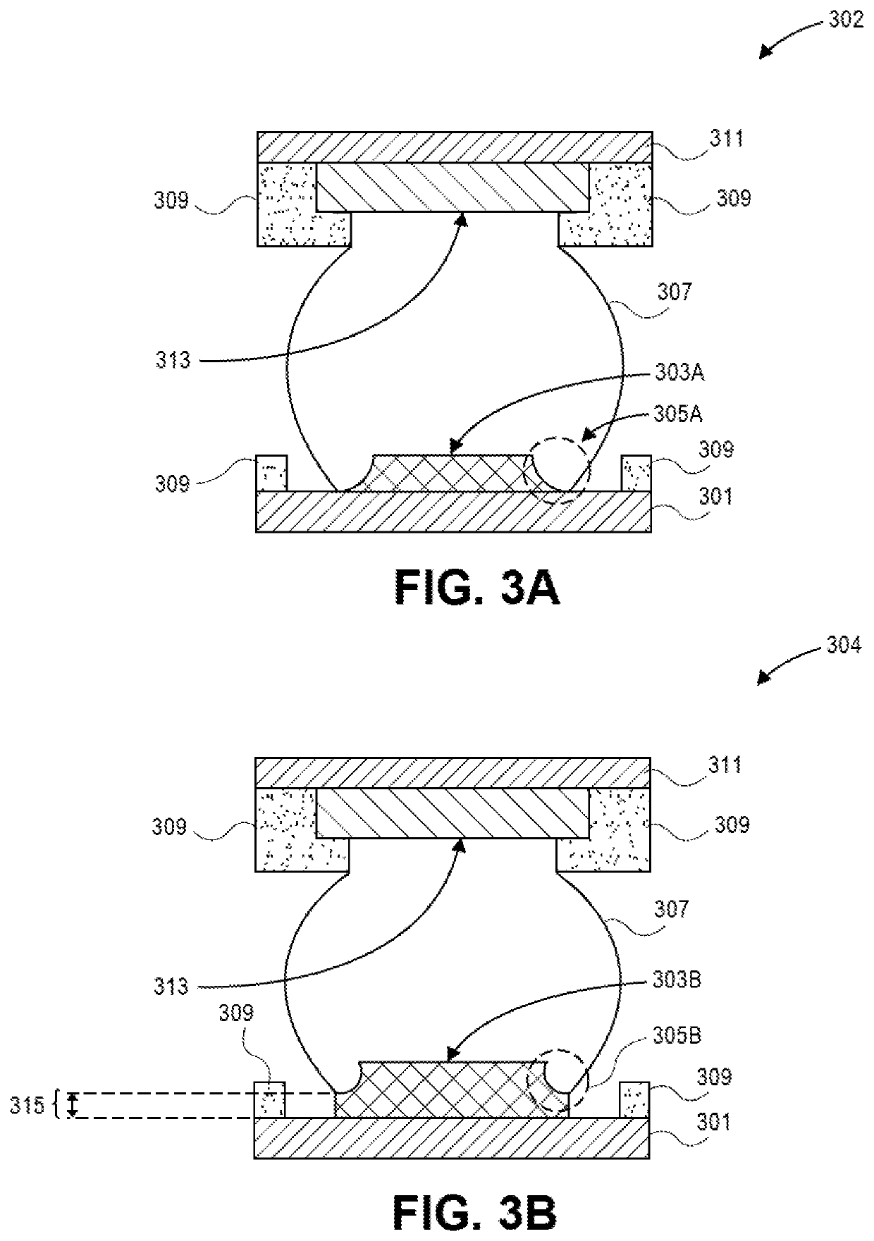
Embodiments described herein provide techniques for forming an interconnect structure that includes micro features formed therein. Such embodiments can assist with improving interconnect joint reliability when compared to conventional pads that have a flat surface. An interconnect structure may comprise: a metal pad over a substrate (e.g., a semiconductor package, a PCB, an interposer, etc.). Micro features may be formed in an edge of the metal pad or away from the edge of the metal pad. The micro features can assist with: (i) increasing the contact area between solder used to form an interconnect joint and the metal pad; and (ii) improving adherence of solder used to form an interconnect joint to the metal pad. These benefits can improve interconnect joint reliability by, among others, improving the interconnect joint's ability to absorb stress from substrates having differing coefficients of thermal expansion.

Description

BACKGROUNDField[0001]Embodiments described herein generally relate to substrates (e.g., semiconductor packages, printed circuit boards (PCB), etc.). More particularly, but not exclusively, embodiments described herein relate to an interconnect structure that is on or part of a substrate.Background Information[0002]At least one packaged system includes a semiconductor package coupled to a PCB. Pressures to improve the performance capabilities of these systems have caused the number of semiconductor dies in a semiconductor package to increase over time. One example of such a package is a package comprised of stacked dies (e.g., memory dies, etc.). Dies are formed from silicon. Hence, as dies in a package increase, the amount of silicon in the package also rises. Increasing silicon in a package, however, reduces the package's overall coefficient of thermal expansion (CTE).[0003]The pressures alluded to above have also led to increased input / output (I / O) density in PCBs, which results f...

Claims


Application Information

Patent Timeline
IPC IPC(8): H01L23/00
CPCH01L2224/0401H01L2224/0361H01L2224/16227H01L24/03H01L24/16H01L2224/05557H01L2924/15323H01L24/05H05K1/111H01L2224/16238H01L2224/05647H01L2224/1329H01L2224/133H01L2224/81815H01L2224/81191H01L2224/81385H01L2224/03831H01L2224/0384H01L2224/03632H01L24/13H01L2224/1607H01L23/49811H01L23/49816H01L2224/05567H01L2224/13147H01L2224/13144H01L2224/13022H05K3/3436H05K3/4007H01L2924/00014H01L2924/0665
Inventor GOGINENI, SIREESHAXU, YICAI, YUHONG
Owner INTEL CORP
Learn More