Masking structure for a wafer supporting plate

a supporting plate and masking technology, applied in the direction of basic electric elements, electrical equipment, electric discharge tubes, etc., can solve the problems reducing the fees for washing the supporting plate, and prolonging the life of the carrying tray 30. , the effect of reducing the risk of product damag

Inactive Publication Date: 2020-04-16
SKYTECH
View PDF3 Cites 1 Cited by
  • Summary
  • Abstract
  • Description
  • Claims
  • Application Information

AI Technical Summary

Benefits of technology

[0004]Accordingly, the object of the present invention is to provide a masking structure for a wafer supporting plate, wherein by using the structure of the present invention, due to the masking effect of the mask 60, in sputtering operation, the film from sputtering will not deposit on the carrying tray 30, while it only deposits on the wafers 32 through the through holes 62 of the mask 60. Therefore, the lifetime of the carrying tray 30 is prolonged greatly and the fees for washing the carrying tray 30 is reduced. Furthermore the risk of destroy of the products is also decreased.

Problems solved by technology

Furthermore the risk of destroy of the products is also decreased.

Method used


Image

  • Masking structure for a wafer supporting plate
  • Masking structure for a wafer supporting plate
  • Masking structure for a wafer supporting plate

Examples


Embodiment Construction

[0013]In order that those skilled in the art can further understand the present invention, a description will be provided in the following in details. However, these descriptions and the appended drawings are only used to cause those skilled in the art to understand the objects, features, and characteristics of the present invention, but not to be used to confine the scope and spirit of the present invention defined in the appended claims.

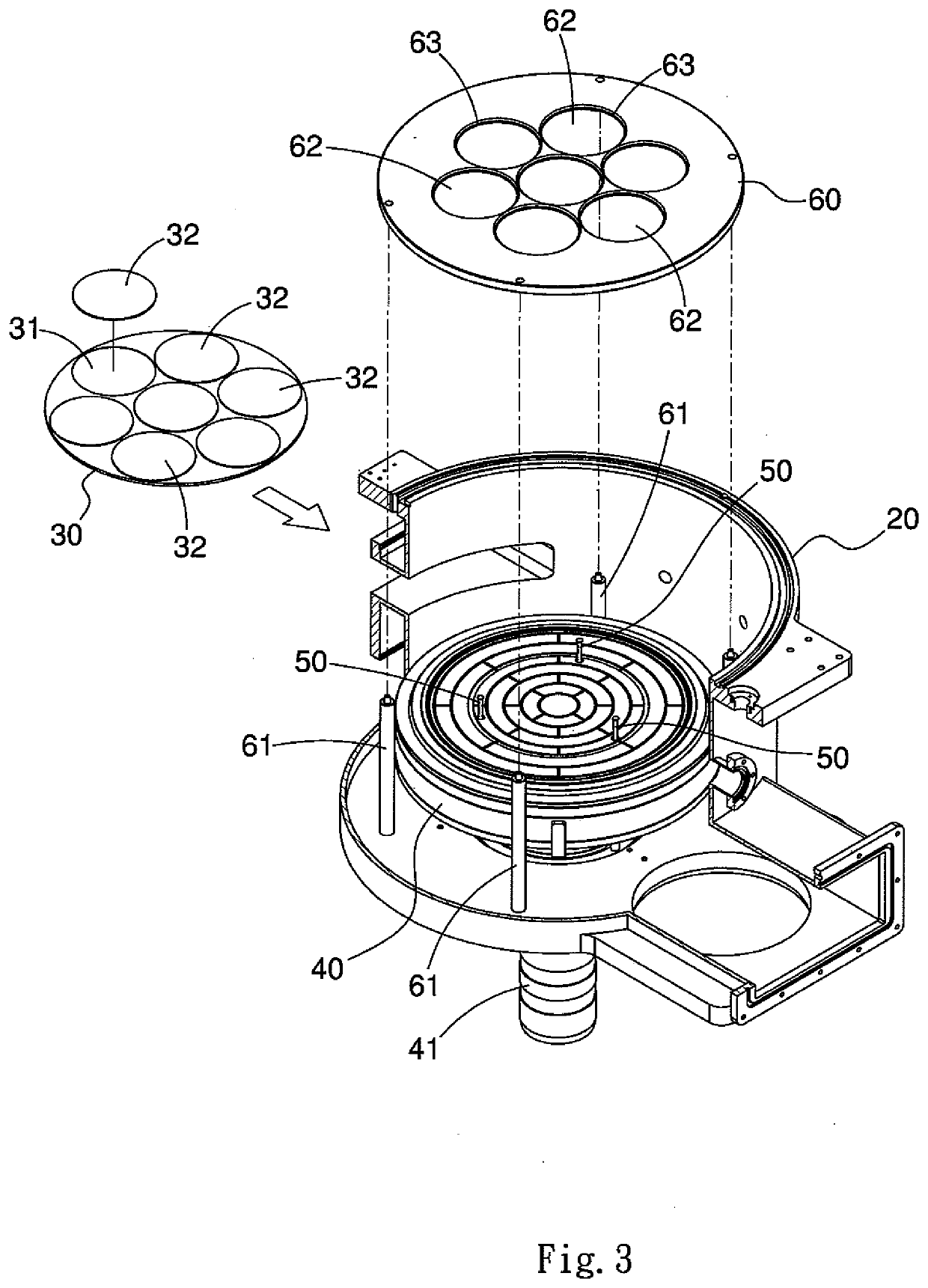
[0014]With reference to FIGS. 3 to 7, the structure of the present invention includes the following elements.

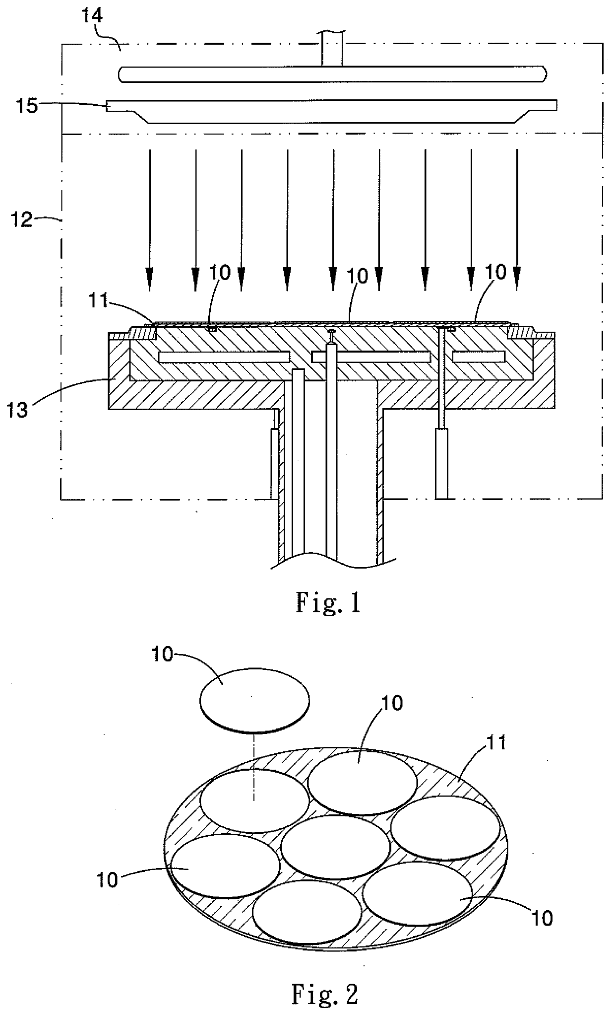
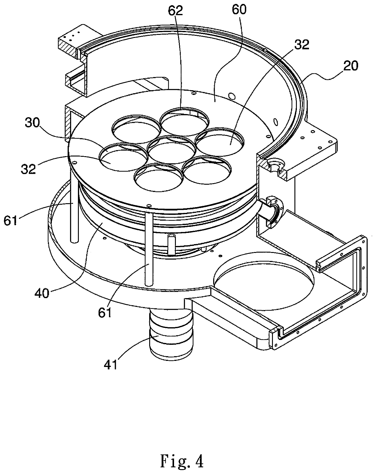
[0015]A cavity 20 is included.

[0016]A carrying tray 30 has a plurality of recesses 31 in a top surface thereof for receiving a plurality of wafers 32. The carrying tray 30 can be transferred into and out of the cavity 20 by using a robot (not shown).

[0017]A supporting plate 40 is installed within the cavity 20 and below the carrying tray. The supporting plate 40 could move upwards, and downwards. A bottom side of the supporting plate 40 is i...


PUM


Abstract

A masking structure for a wafer supporting plate comprises a cavity; a carrying tray having a plurality of recesses in a top surface thereof for receiving a plurality of wafers; the carrying tray can be transferred into and out of the cavity by using a robot; a supporting plate installed within the cavity and below the carrying tray; the supporting plate could move upwards, and downwards; a mask installed within the cavity and above the carrying tray; the mask formed with a plurality of through holes which are positioned and shaped to be corresponding to those of the wafers on the carrying tray; therefore, when the supporting plate lifts the carrying tray to be near the mask, the wafers are exposed out of the through holes.

Description

FIELD OF THE INVENTION[0001]The present invention relates to wafer manufacturing process, in particular to a masking structure for a wafer supporting plate.BACKGROUND OF THE INVENTION[0002]Referring to FIGS. 1 and 2, in plating of films in general semiconductor packaging processes, LED packaging processes, and panel manufacturing processes, for increasing the production rate, generally, the wafers 10 are placed in a carrying tray 11 which is then transferred to a supporting plate 13 of a cavity 12 by using a robot. Then a sputtering device 14 at an upper side of the cavity 12 will sputter atoms from a target so that the atoms are deposited on the wafers 10.[0003]However, in the plating process, the sputtering of atom will pollute the supporting plate 11 locating the wafers 10 (referring to a dashed area in FIG. 2). With the times of plating, the deposited films on the supporting plate will become thicker and thicker so as to induce peeling pollution and particles pollution. Although...

Claims


Application Information

Patent Timeline
Patent Type & Authority Applications(United States)
IPC IPC(8): H01J37/34H01L21/687H01J37/32
CPCH01J37/32715H01L21/68771H01J37/3441H01L21/68721H01L21/68742H01L21/67754
Inventor LU, LIN-SHENGHSIEH, CHENG-CHIHCHEN, HSUAN-CHUNGCHIU, HSIN CHIHCHENG, YAO-SYUANWANG, CHUN-FU
Owner SKYTECH
Why Eureka
Try Eureka