
Coating material for processing chambers

Pending Publication Date: 2020-02-20
APPLIED MATERIALS INC
View PDF3 Cites 1 Cited by
  • Summary
  • Abstract
  • Description
  • Claims
  • Application Information

AI Technical Summary

Benefits of technology

This patent describes coating materials with high electrical resistivity for use in substrate processing chambers. The high resistivity layer is a layer of material that is deposited on the surface of a chamber component and has a very high electrical resistance. This helps to prevent electrical arcing and other issues that can occur when manufacturing semiconductor devices. The methods for depositing the coating involve applying a high pressure, power, and temperature while using different gases and flow rates. The use of this coating results in improved safety and efficiency during substrate processing.

Problems solved by technology

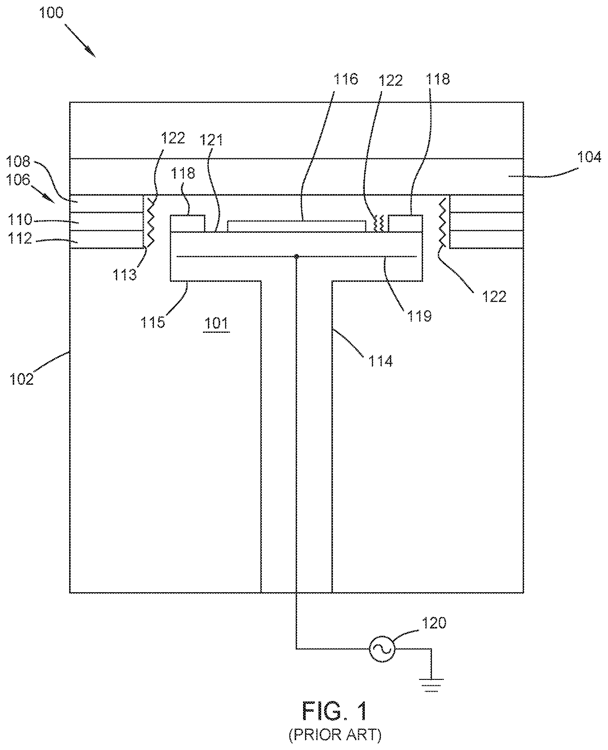
As higher charges are created at the top surface of the thermal conductive support, it exposes the thermal conductive support to more electrical arcing incidents.
These arcing incidents can also occur on the surfaces of the chamber walls, the process kit stacks, and / or other chamber components during processing.
Arcing events result in particle contamination, wafer scrap, yield loss, and chamber downtime.
Additionally, when direct current (DC) voltage is applied to the thermal conductive support for electrostatic chucking, the leakage current in the thermal conductive support causes charges generated by the DC voltage to leak out of the thermal conductive support during plasma processing.
This results in an unstable chucking performance leading to chucking degradation.

Method used


Image

  • Coating material for processing chambers
  • Coating material for processing chambers
  • Coating material for processing chambers

Examples


Embodiment Construction

[0018]In the following description, numerous specific details are set forth to provide a more thorough understanding of the embodiments of the present disclosure. However, it will be apparent to one of skill in the art that one or more of the embodiments of the present disclosure may be practiced without one or more of these specific details. In other instances, well-known features have not been described in order to avoid obscuring one or more of the embodiments of the present disclosure.

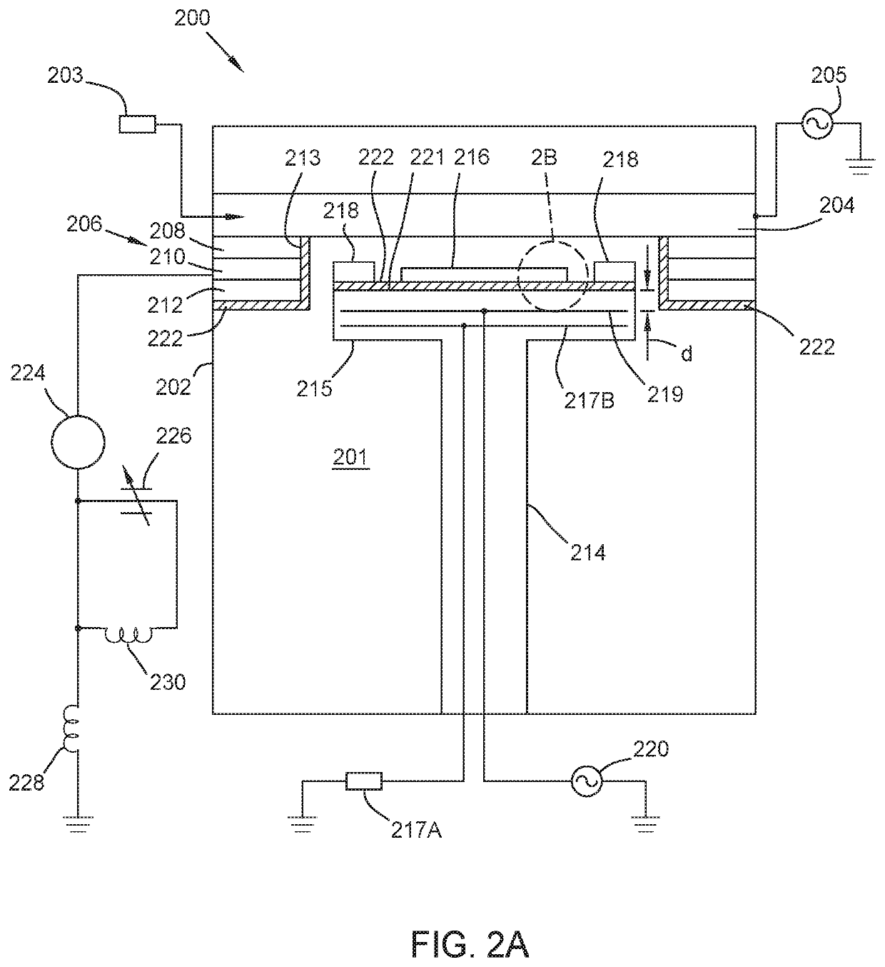
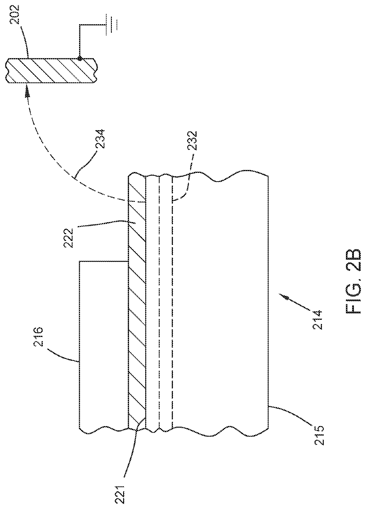
[0019]Embodiments described herein generally relate to process chamber components that include a coating that has a high electrical resistivity for use in plasma processing. As higher temperature and higher plasma density processes are developed for processing semiconductor substrates, higher amounts of charge can be created and trapped with the various exposed processing chamber components, such as at the top surface of a thermal conductive support disposed within a processing region of the proces...


PUM

PropertyMeasurementUnit
Temperatureaaaaaaaaaa
Thicknessaaaaaaaaaa
Pressureaaaaaaaaaa

Abstract

Embodiments described herein relate to coating materials with high resistivity for use in processing chambers. To counteract the high charges near the top surface of the thermal conductive support, the top surface of the thermal conductive support can be coated with a high resistivity layer. The high resistivity of the layer reduces the amount of charge at the top surface of the thermally conductive element, greatly reducing or preventing arcing incidents along with reducing electrostatic chucking degradation. The high resistivity layer can also be applied to other chamber components. Embodiments described herein also relate to methods for fabricating a chamber component for use in a processing environment. The component can be fabricated by forming a body of a chamber component, optionally ex-situ seasoning the body, installing the chamber component into a processing chamber, in-situ seasoning the chamber component, and performing a deposition process in the processing chamber.

Description

CROSS-REFERENCE TO RELATED APPLICATIONS[0001]This application claims priority to U.S. Provisional Patent Application No. 62 / 719,575, filed Aug. 17, 2018, which is herein incorporated by reference in its entirety.BACKGROUNDField[0002]Embodiments described herein generally relate to coating materials for use in processing chambers and, more particularly, to coating materials having a high electrical resistivity for use in processing chambers.Description of the Related Art[0003]Semiconductor processing apparatuses typically include a process chamber that is adapted to perform various deposition, etching, or thermal processing steps on a wafer, or substrate, that is supported within a processing region of the process chamber. Gases are provided in a processing region of the process chamber. The gases become “excited” by the delivery of RF energy, transitioning the gases into a plasma state, thereafter forming a layer on the surface of the wafer. Typically, the wafer is supported by a wa...

Claims


Application Information

Patent Timeline
IPC IPC(8): H01L21/687H01L21/683C23C16/458C23C16/46C23C16/50C23C16/40
CPCC23C16/4586H01L21/6833C23C16/401C23C16/50C23C16/46H01L21/68735H01L21/68757H01L21/6831H01L21/67103C23C16/4404C23C16/4581H01L21/67017H01L21/6835H01L21/0226H01L21/02312
Inventor RATHI, SUDHALEE, DONG HYUNGKHAJA, ABDUL AZIZBALASUBRAMANIAN, GANESHROCHA, JUAN CARLOS
Owner APPLIED MATERIALS INC
Learn More