
High-frequency module and communication device

a communication device and high-frequency module technology, applied in waveguide devices, high-frequency circuit adaptations, printed circuit non-printed electric components association, etc., can solve problems such as deteriorating the circuit characteristics of high-frequency modules, and achieve excellent circuit characteristics and high-frequency noise suppression. , excellent

Active Publication Date: 2020-02-06
MURATA MFG CO LTD
View PDF0 Cites 0 Cited by
  • Summary
  • Abstract
  • Description
  • Claims
  • Application Information

AI Technical Summary

Benefits of technology

The present disclosure pertains to a high-frequency module and a communication device that can suppress high-frequency noise and have excellent circuit characteristics. This will result in a high-frequency module and a communication device that have high-frequency noise suppression and good circuit performance.

Problems solved by technology

However, in some cases, a shielding conductor film forms an unintended signal path in the high-frequency module (specifically, between a plurality of circuits provided in the high-frequency module) and deteriorates the circuit characteristics of the high-frequency module.

Method used


Image

  • High-frequency module and communication device
  • High-frequency module and communication device
  • High-frequency module and communication device

Examples


first embodiment

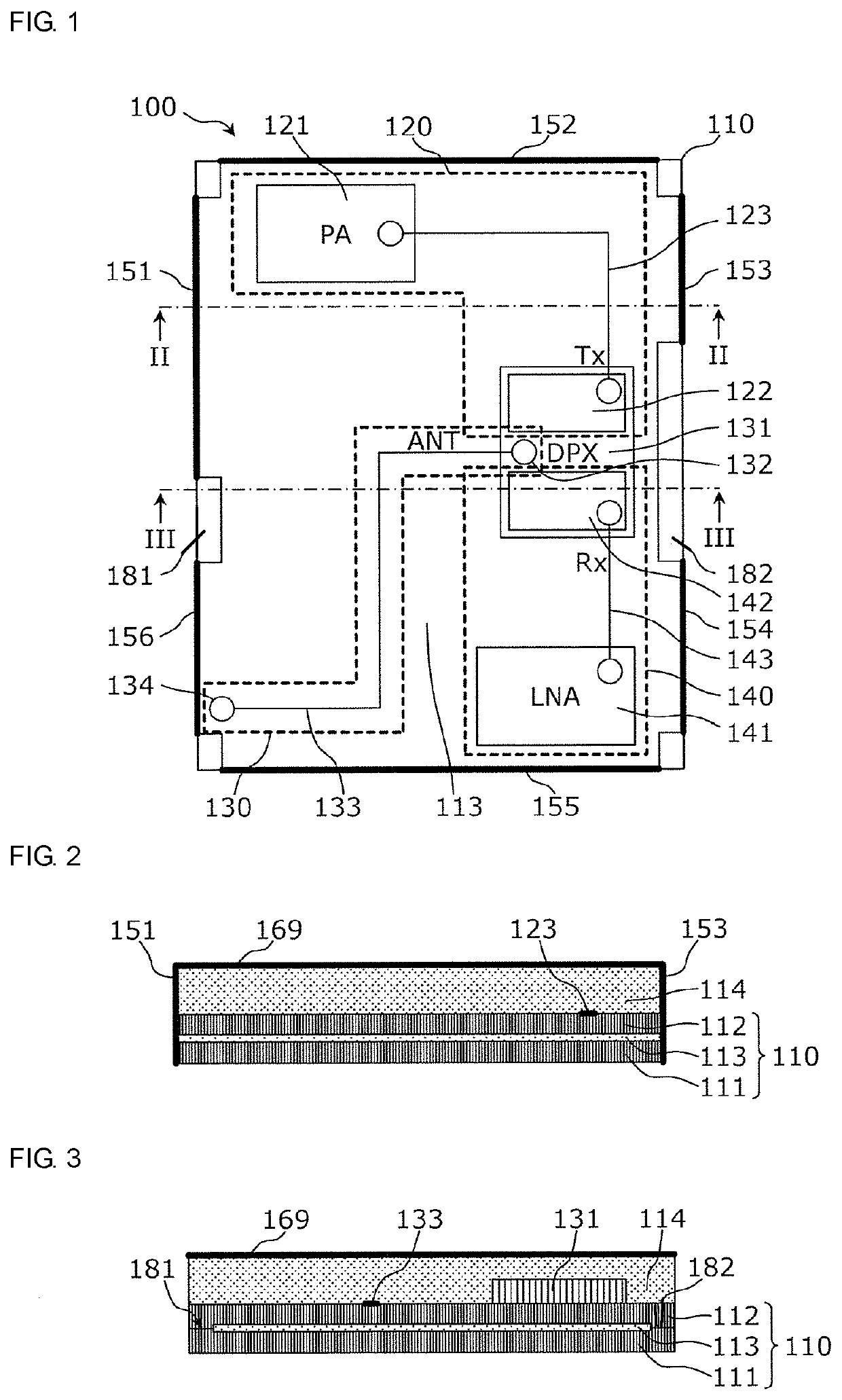
[0032]FIG. 1 is a plan view illustrating an example of a structure of a high-frequency module according to a first embodiment.

[0033]FIGS. 2 and 3 are cross-sectional views illustrating an example of the structure of the high-frequency module according to the first embodiment. The cross-sectional view in FIG. 2 corresponds to a cross section taken along line II-II in FIG. 1 as viewed in the direction of the arrows, and the cross-sectional view in FIG. 3 corresponds to a cross section taken along line III-III in FIG. 1 as viewed in the direction of the arrows.

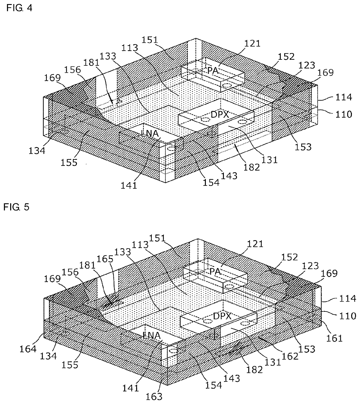
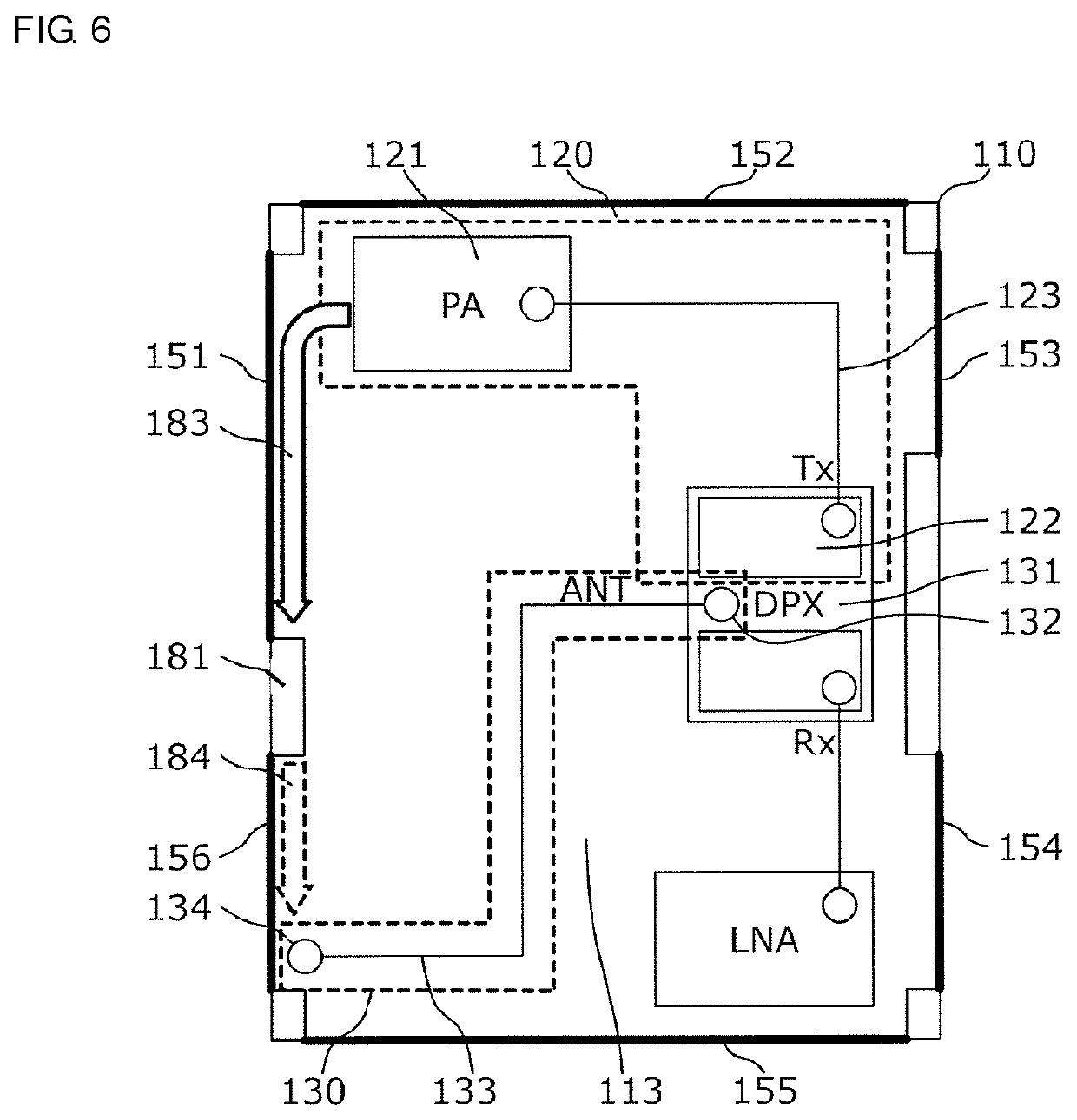
[0034]As illustrated in FIGS. 1 to 3, a high-frequency module 100 includes a power amplifier 121, a duplexer 131, and a low noise amplifier 141 that are mounted on a multilayer board 110, and includes a connection terminal 134 for inputting and outputting antenna signals.

[0035]The power amplifier 121 and the duplexer 131 are connected with a wiring pattern 123. The duplexer 131 and the connection terminal 134 are connected with a...

second embodiment

[0084]In a second embodiment, a communication device will be described that includes a front-end circuit including the high-frequency module according to the first embodiment.

[0085]FIG. 8 is a block diagram illustrating an example of a functional configuration of a communication device 1 according to the second embodiment. As illustrated in FIG. 8, the communication device 1 includes a front-end circuit 10, an RF signal processing circuit 20, and a baseband signal processing circuit 30.

[0086]The front-end circuit 10 includes a power amplifier 11, a low noise amplifier 12, and a duplexer 13. For the front-end circuit 10, the high-frequency module 100 described in the first embodiment is used.

[0087]In the front-end circuit 10, the power amplifier 11 amplifies a transmission RF signal Tx received from the RF signal processing circuit 20.

[0088]The duplexer 13 supplies the transmission RF signal Tx amplified by the power amplifier 11 to an antenna circuit and also supplies a reception RF...


PUM


Abstract

A high-frequency module (100) includes a multilayer board (110) including a plurality of insulator layers and at least one ground conductor layer (113); in the multilayer board (110), a transmission circuit (120) that is a first circuit provided in a first region and an antenna circuit (130) that is a second circuit provided in a second region different from the first region; and shielding conductor films (151 to 156) provided on sides of the multilayer board (110) and being partially in contact with the ground conductor layer (113). The ground conductor layer (113) is not in contact with the shielding conductor films (151 to 156) in, of a side of the multilayer board (110), a portion that is closest both to the first region and to the second region.

Description

[0001]This is a continuation of International Application No. PCT / JP2018 / 019336 filed on May 18, 2018 which claims priority from Japanese Patent Application No. 2017-110366 filed on Jun. 2, 2017. The contents of these applications are incorporated herein by reference in their entireties.BACKGROUND OF THE DISCLOSUREField of the Disclosure[0002]The present disclosure relates to a high-frequency module and a communication device.Description of the Related Art[0003]In the related art, there is a high-frequency module (for example, Patent Document 1) including a plurality of electronic components mounted on an upper surface of a printed circuit board, a resin portion covering the plurality of electronic components, a shielding metal film formed on at least a part of a side of the printed circuit board and a surface of the resin portion, and a ground pattern connected to the shielding metal film at the side of the printed circuit board. The shielding metal film keeps high-frequency noise ...

Claims


Application Information

Patent Timeline
IPC IPC(8): H04B1/50H04B1/00H01L23/28H01L23/538H01L23/66H05K1/18H01P1/20H05K1/02H05K9/00
CPCH01L23/5383H01L23/28H05K1/0219H01P1/20H04B1/50H01L23/66H05K1/18H05K9/0039H05K1/0237H04B1/0057H01L23/12H01P1/2135H05K3/284H05K1/0216H05K2203/1322H05K1/0243H01L23/552H01L2223/6677
Inventor NAKAGAWA, DAI
Owner MURATA MFG CO LTD
Learn More