Connection structure

Active Publication Date: 2020-01-02
DEXERIALS CORP
View PDF5 Cites 2 Cited by
  • Summary
  • Abstract
  • Description
  • Claims
  • Application Information

AI Technical Summary

Benefits of technology

The present invention relates to a connection structure for electronic components with terminal patterns. The invention aims to reduce or eliminate terminals that capture no conductive particles, which can improve the reliability and performance of the connection structure. The invention provides methods for achieving this by analyzing the size and arrangement of the terminals, and by optimizing the arrangement of conductive particles in the anisotropic conductive film. These methods can be applied regardless of the size or pitch of the terminals, and can lead to a more symmetrical and effective connection between electronic components.

Problems solved by technology

However, the use of the FPCs and the plastic substrates brings about a problem that the layout of terminals minutely varies even among the same electronic components before anisotropic conductive connection due to the effect of environmental temperature on thermal expansion.
In the case of continuously performing the anisotropic conductive connection in mass production of products in which the electronic components are mounted, if pressure bonding temperature varies in individual connection, there is also a problem that the positions of the terminals tend to deviate from their predetermined positions due to the effect of the pressure bonding temperature on thermal expansion.
Among the electronic components of different production lots, the substrates and the like on which the terminals are provided are sometimes made of materials having different coefficients of linear expansion, so the same problem occurs.
As described above, the problems relating to the thermal expansion of the electronic components exist before and after a connection process.

Method used


Image

  • Connection structure
  • Connection structure
  • Connection structure

Examples


example 1

[0145]In the case of producing a connection structure in which terminal patterns having radially arranged terminals were connected to each other, the number of conductive particles captured by each terminal was determined by overlapping the terminal patterns having the radially arranged terminals and a particle arrangement by drawing figures. The connection structure was determined to be OK when the terminal captured three or more conductive particles at the minimum, and determined to be NG when the terminal captured less than three conductive particles.

[0146]In this case, a first electronic component had a terminal pattern of the following form.

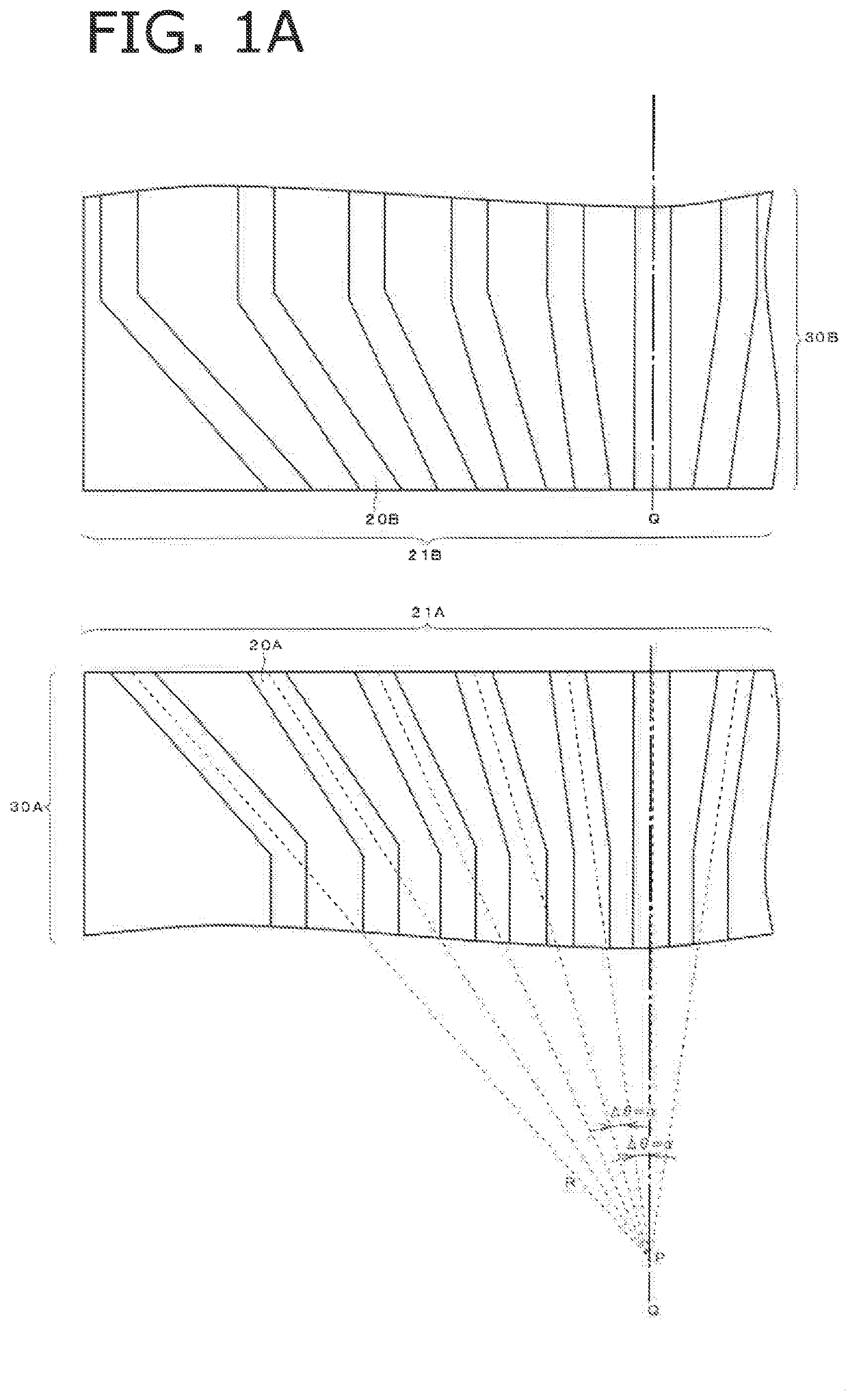
[0147](1) As a terminal pattern 21, as shown in FIG. 8A, a radial arrangement having two terminals was presumed.

[0148](2) The angle α formed between a center line Q of the terminal pattern 21 and a center line R extending in a long-side direction of a terminal 20 was varied by angles of 0.01 to 1°, and a maximum value αmax was set to 14°.

[01...

example 2

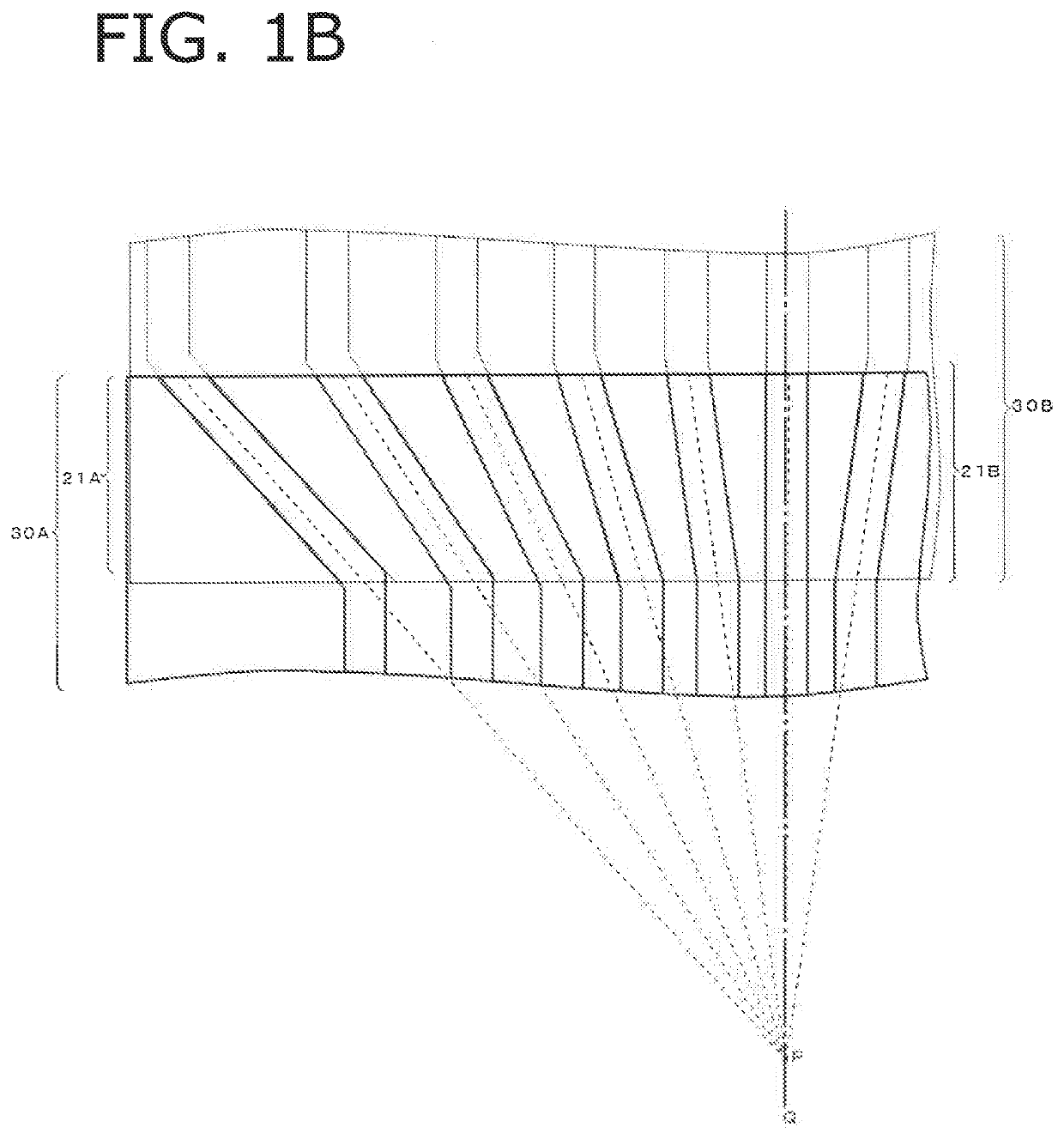
[0157]The number of conductive particles captured by the terminal was determined by drawing figures, using the same terminal pattern as that in Example 1 in the same manner as that in Example 1.

[0158]In an anisotropic conductive film, conductive particles had a particle diameter of 3.2 μm, a square lattice disposition, and an interstitial distance (distance between centers of conductive particles) of 10 μm.

[0159]As a result, in a case where the center line R of the terminal 20 was inclined to the maximum value αmax, the minimum capture number of the conductive particles by the terminal 20 was evaluated to be OK, and there was no instance in which the terminal 20 captured no conductive particles, even if the angle formed between the center line Q and the center line R took any value.

example 3

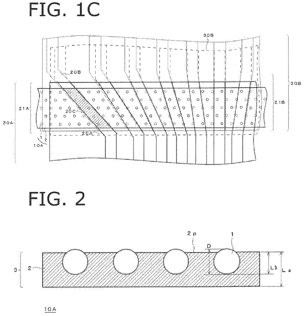
[0162]The number of conductive particles captured by a terminal was determined by drawing figures, using the same terminal pattern as that in Example 1 in the same manner as that in Example 1. However, an anisotropic conductive film had the following conductive particle disposition.

[0163]Namely, the anisotropic conductive film had a multiple circular region illustrated in FIG. 5B. In this case, the multiple circular region had the following specifications.

[0164]The diameter of a first concentric circle was 20 μm.

[0165]The distance L2 between the centers of the conductive particles on each concentric circle was 10 μm.

[0166]The distance L3 between concentric circles was 10 μm.

[0167]The angle θ formed between a first line 23a and a second line 23b was 5°.

[0168]A cutout rectangular region was a square the side of which was 100 μm.

[0169]As a result, the minimum capture number of the conductive particles by the terminal was evaluated to be OK.

[0170]Note that, as illustrated in FIG. 8B, wh...


PUM

PropertyMeasurementUnit
Areaaaaaaaaaaa
Densityaaaaaaaaaa
Electrical conductoraaaaaaaaaa

Abstract

A connection structure: a first electronic component having a terminal pattern in which a plurality of terminals are arranged side by side in a radial form and a second electronic component having a terminal pattern corresponding to the terminal pattern of the first electronic component are anisotropically conductively connected using an anisotropic conductive film, (i) the effective connection area per terminal is 3000 μm2 or more, and the number density of conductive particles in the anisotropic conductive film is 2000 particles / mm2 or more and 20000 particles / mm2 or less, (ii) as the anisotropic conductive film, adopted is an anisotropic conductive film in which the conductive particles are arranged in a lattice form, and the arrangement pitch and the arrangement direction are configured such that each terminal captures three or more conductive particles, or (iii) as the anisotropic conductive film, adopted is an anisotropic conductive film having a multiple circular region.

Description

TECHNICAL FIELD[0001]The present invention relates to a connection structure using an anisotropic conductive film.BACKGROUND ART[0002]In electronic components such as IC chips, terminal pitches are becoming finer. With reduction in weight of the electronic components, FPCs (flexible printed circuits) and plastic substrates having relatively low specific gravities are often used. To mount the electronic components, an anisotropic conductive film, in which conductive particles are dispersed in an insulating resin layer, is widely used.[0003]However, the use of the FPCs and the plastic substrates brings about a problem that the layout of terminals minutely varies even among the same electronic components before anisotropic conductive connection due to the effect of environmental temperature on thermal expansion. In the case of continuously performing the anisotropic conductive connection in mass production of products in which the electronic components are mounted, if pressure bonding ...

Claims


Application Information

Patent Timeline
IPC IPC(8): H05K3/32C08L101/00H01B5/16H01R11/01H01R43/20C09J9/02C09J7/20
CPCH01R11/01C08K2201/005H05K3/323C08L101/00C09J2205/102C09J2201/36C09J7/20H01B5/16C09J9/02C09J2201/602H01R43/20C09J5/00C09J7/10C09J2203/326C08K2201/001H01L2224/83101H05K3/368H05K2201/0269C09J2301/314C09J2301/408C09J2301/208
Inventor ARAKI, YUTA
Owner DEXERIALS CORP
Why Eureka
Try Eureka