
Method for manufacturing gi optical waveguide

Pending Publication Date: 2020-01-02
KEIO UNIV +1
View PDF0 Cites 0 Cited by
  • Summary
  • Abstract
  • Description
  • Claims
  • Application Information

AI Technical Summary

Benefits of technology

The present invention provides a method for making an optical waveguide with a circular core, which helps reduce insertion loss.

Problems solved by technology

Thus, problems have become apparent in data servers in which transmitted information data are concentrated; for example, the data servers use a huge amount of electricity, and the processing capacities of the data servers have almost reached their limits.
However, a GI optical waveguide is considerably difficult to manufacture, and only a few manufacturing methods therefor have been reported.

Method used


Image

  • Method for manufacturing gi optical waveguide
  • Method for manufacturing gi optical waveguide
  • Method for manufacturing gi optical waveguide

Examples


example 2

[Manufacturing Example 2] Manufacturing of Reactive Silicone Compound (SC2)

[0106]A 200 mL eggplant-shaped flask equipped with a condenser and a Dean-Stark apparatus was charged with 43.3 g (0.20 mol) of DPSD, 44.9 g (0.20 mol) of STMS, and 35 g of toluene, and air in the flask was purged with nitrogen by using a nitrogen balloon. The reaction mixture was heated to 50° C., and then 38 mg (0.2 mmol) of barium hydroxide monohydrate [available from Aldrich] was added to the flask. The mixture was stirred at 50° C. for one hour, and then further heated to 85° C. Thereafter, while by-produced methanol was removed to the outside of the reaction system, the mixture was stirred for five hours for dealcoholization condensation. The resultant reaction mixture was cooled to room temperature (about 23° C.), and insoluble matter was removed with a membrane filter having a pore size of 0.2 μm. Toluene was distilled off from the reaction mixture with a rotary evaporator under reduced pressure at 50...

example 3

[Manufacturing Example 3] Preparation of Curable Composition 1

[0108]98.6 Parts by mass of SC1 manufactured in Manufacturing Example 1, 1.4 parts by mass of DVB, and 1 part by mass of TPO were mixed together with stirring at 50° C. for three hours. The mixture was further stirred and defoamed for two minutes to thereby prepare curable composition 1.

[0109]The resultant composition was found to have a viscosity of 51,300 mPa·s at 25° C.

examples 4 to 6

[Manufacturing Examples 4 to 6] Preparation of Curable Compositions 2 to 4

[0110]Curable compositions 2 to 4 shown in Table 1 were prepared in the same manner as in Manufacturing Example 3. The viscosities of the resultant compositions at 25° C. are also shown in Table 1.

TABLE 1SC1SC2DVBDOGTPOI127[Parts[Parts[Parts[Parts[Parts[PartsbybybybybybyViscositymass]mass]mass]mass]mass]mass][mPa · s]Curable98.61.4151,300composition 1Curable87.512.5119,000composition 2Curable93.066.9434,700composition 3Curable7525113,800composition 4


PUM


Abstract

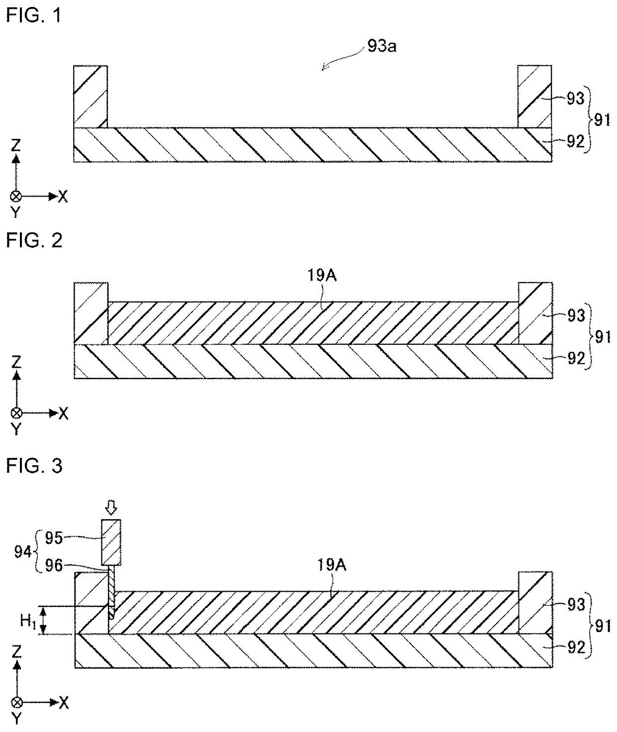
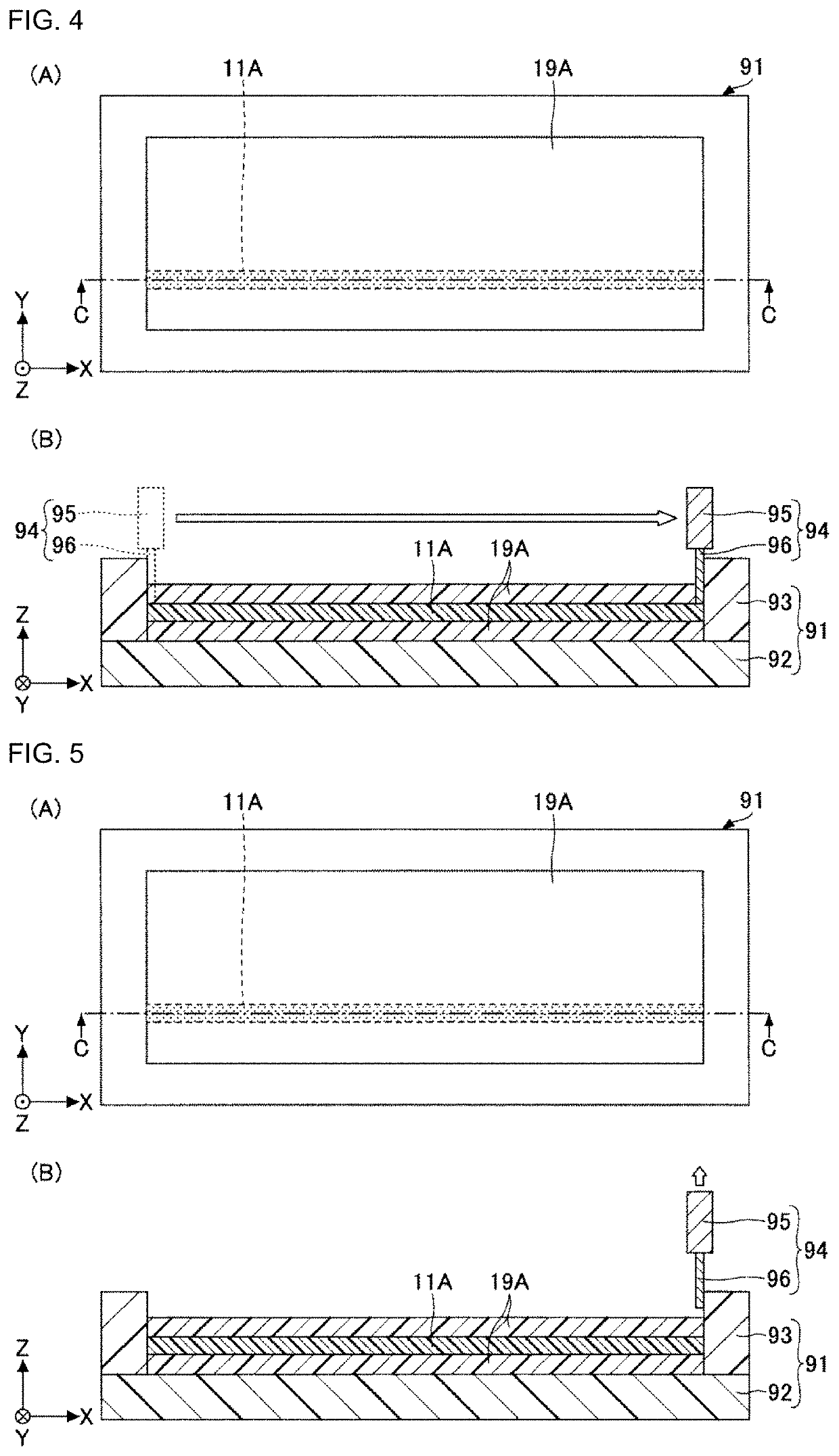
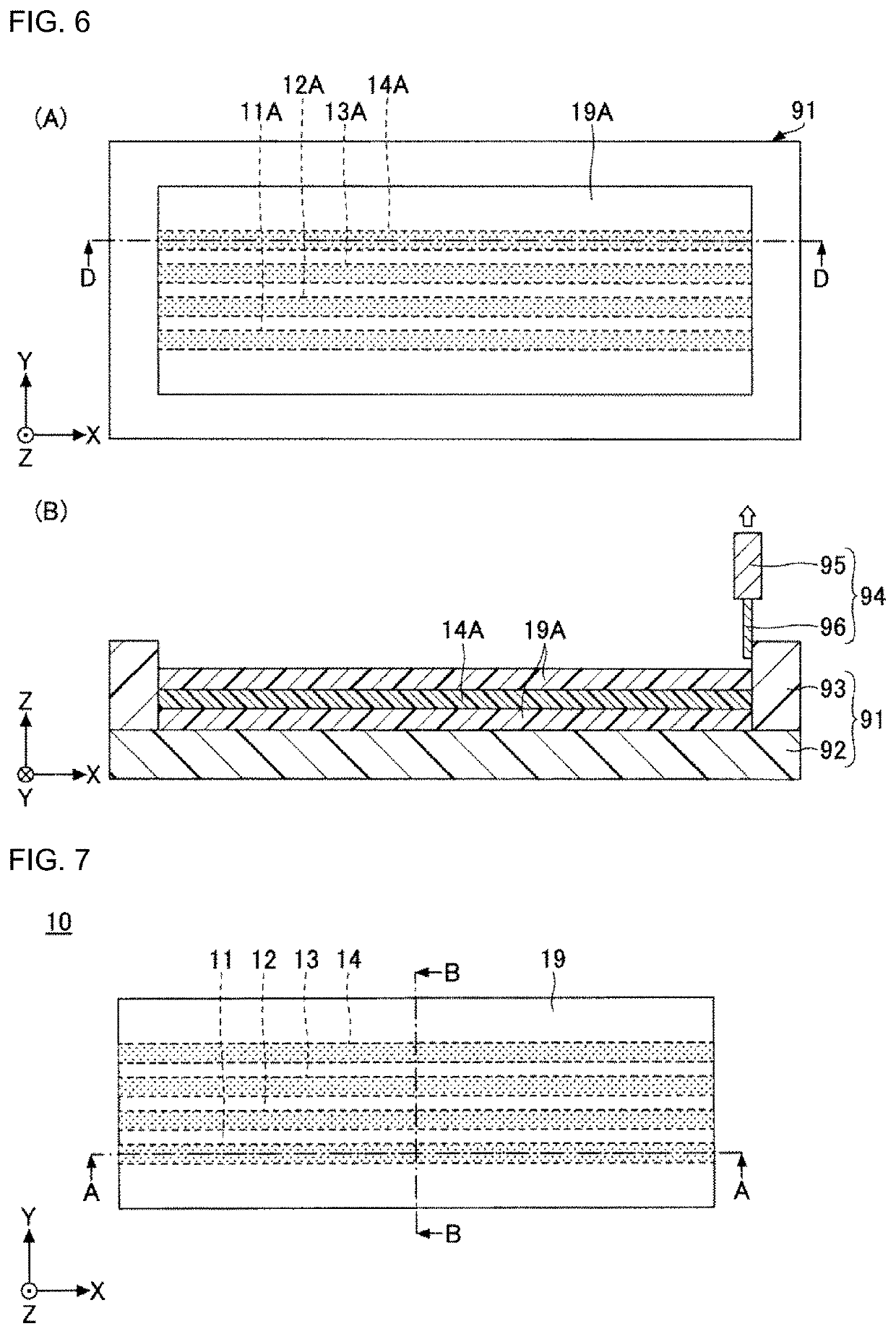
A GI optical waveguide includes a core having a substantially circular cross-sectional shape. A method for manufacturing an optical waveguide, includes a first step of inserting an acicular section at the tip of a discharge unit into an uncured cladding; a second step of moving the acicular section within the uncured cladding while discharging an uncured material from the acicular section, to thereby form an uncured core surrounded by the uncured cladding; a third step of removing the acicular section from the uncured cladding; and a fourth step of curing the uncured cladding and the uncured core, wherein: the ratio of the viscosity of the material for forming the uncured core to the viscosity of the uncured cladding is 1.20 to 6 at the temperature in the second step.

Description

TECHNICAL FIELD[0001]The present invention relates to a method for manufacturing a GI optical waveguide, more particularly to a method for manufacturing a GI optical waveguide including a core having a substantially circular cross-sectional shape.BACKGROUND ART[0002]In recent years, communication traffic has been increasing as a result of the development of cloud computing and an increase in the number of smartphone users. Thus, problems have become apparent in data servers in which transmitted information data are concentrated; for example, the data servers use a huge amount of electricity, and the processing capacities of the data servers have almost reached their limits. Therefore, technical development is urgently needed for solving such problems. In this situation, vigorous attempts have been made to develop a technique regarding an optoelectronic hybrid substrate (also referred to as “optoelectronic composite substrate”) wherein electrical wiring is partially replaced by optic...

Claims


Application Information

Patent Timeline
IPC IPC(8): B29D11/00G02B6/02
CPCB29D11/00682G02B6/02038G02B6/138G02B6/122G02B6/13
Inventor ISHIGURE, TAKAAKISAITO, YUKIMARUSHIMA, CHINAMINAGASAWA, TAKEHIRO
Owner KEIO UNIV
Learn More