
Physics module of chip-scale atomic clock

a chip-scale atomic clock and module technology, applied in the field of atomic clocks, can solve the problems of increasing the volume and power consumption of the physics module of the general chip-scale atomic clock, and the inability to adopt polarization beam splitters to the chip, so as to reduce the volume and power consumption of the physics module

Active Publication Date: 2019-11-14
KOREA RES INST OF STANDARDS & SCI
View PDF2 Cites 1 Cited by
  • Summary
  • Abstract
  • Description
  • Claims
  • Application Information

AI Technical Summary

Benefits of technology

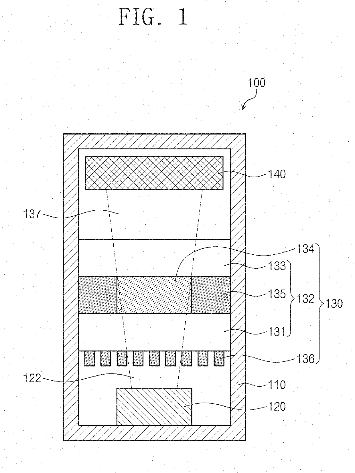
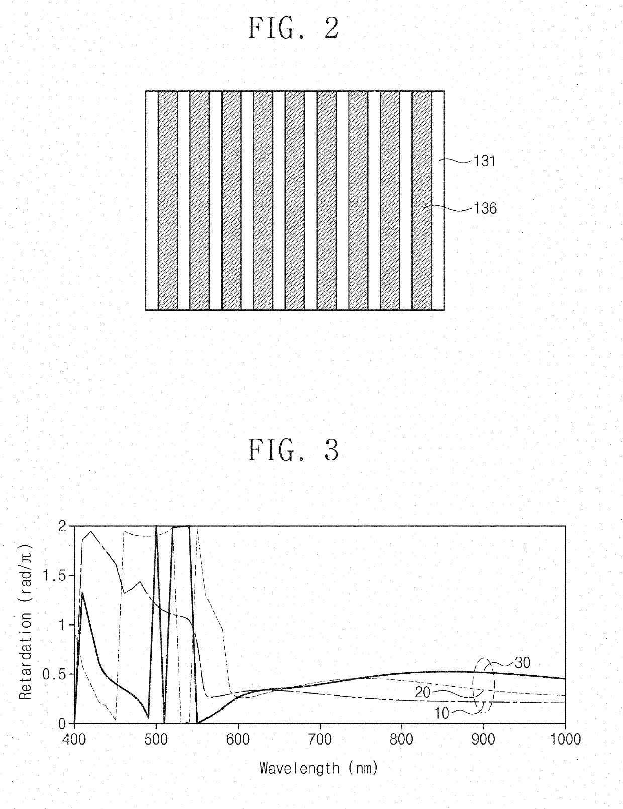
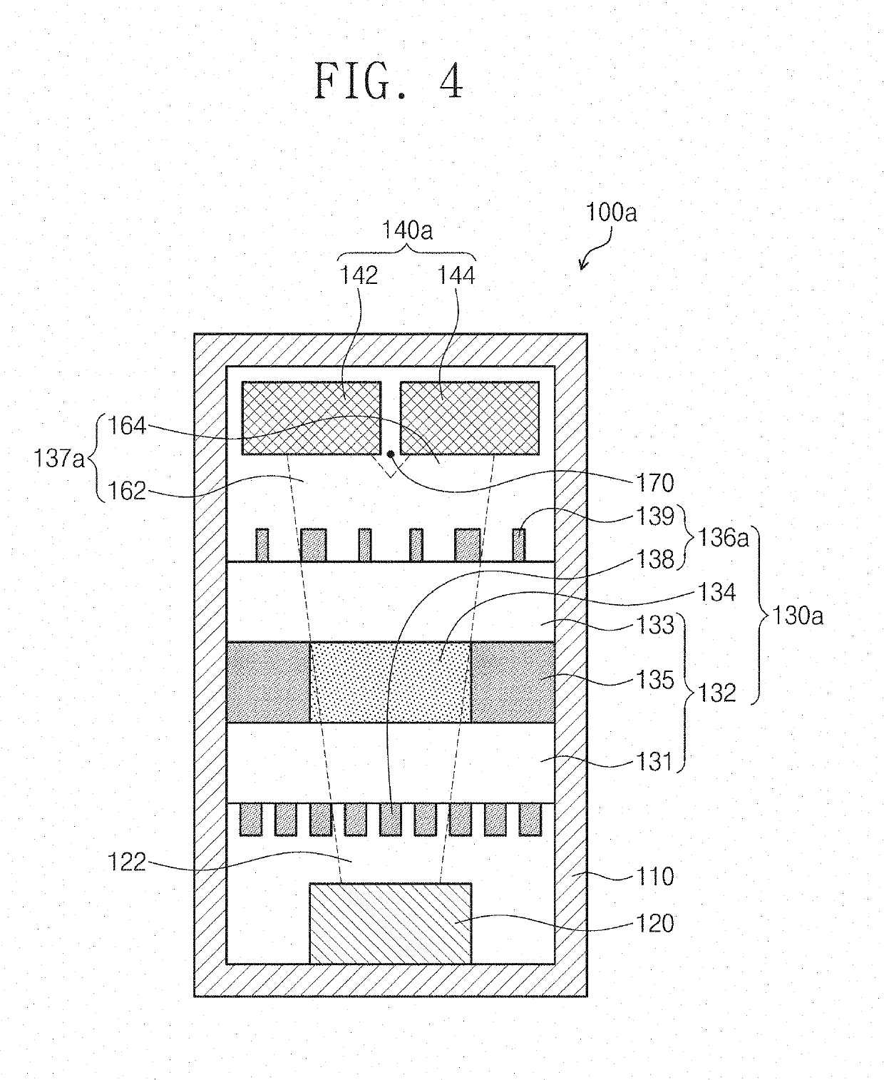
The patent describes a new design for a chip-scale atomic clock that uses optical patterns on the inner and outer walls of a vapor cell. These patterns are thinner than typical parts, which reduces the amount of power needed to maintain a consistent temperature. This design helps to make the whole device more compact and power-efficient.

Problems solved by technology

However, the quarter wave plate and / or the polarization beam splitter increase the volume and consumed power of the physics module of the general chip-scale atomic clock.
For example, the polarization beam splitter has not been adopted to the chip-scale atomic clock due to a required space and power thereof.

Method used


Image

  • Physics module of chip-scale atomic clock
  • Physics module of chip-scale atomic clock
  • Physics module of chip-scale atomic clock

Examples


Embodiment Construction

[0030]Hereinafter, preferred embodiments of the inventive concept will be described below in detail with reference to the accompanying drawings. Advantages and features of the present invention, and implementation methods thereof will be clarified through following embodiments described with reference to the accompanying drawings. The present invention may, however, be embodied in different forms and should not be construed as limited to the embodiments set forth herein. Rather, these embodiments are provided so that this disclosure will be thorough and complete, and will fully convey the scope of the present invention to those skilled in the art. Like reference numerals refer to like elements throughout.

[0031]In the following description, the technical terms are used only for explaining a specific exemplary embodiment while not limiting the present disclosure. The terms of a singular form may include plural forms unless referred to the contrary. The meaning of “include,”“comprise,”...


PUM


Abstract

An embodiment of the inventive concept provides a physics module of a chip-scale atomic clock. The physics module includes: a housing; a laser source disposed in the housing and generating a laser beam; a vapor cell disposed above the laser source to generate a transmitted beam from the laser beam; and a detector disposed above the vapor cell to detect the transmitted beam. Here, the vapor cell may include a plurality of optical patterns configured to polarize the laser beam.

Description

CROSS-REFERENCE TO RELATED APPLICATIONS[0001]This U.S. non-provisional patent application claims priority under 35 U.S.C. § 119 of Korean Patent Application No. 10-2017-0000424, filed on Jun. 7, 2019, the entire contents of which are hereby incorporated by reference.TECHNICAL FIELD[0002]The present disclosure herein relates to an atomic clock, and particularly, to a physics module of a chip-scale atomic clock.BACKGROUND ART[0003]In general, an atomic clock is a device using energy levels of the ground state of alkali vapor as a frequency standard. The alkali vapor may absorb a portion of a laser beam having a resonant frequency. The portion of the laser beam may pass through the alkali vapor and constitutes a transmitted beam. The incident laser beam and the transmitted beam may have a plurality of side band spectra by current modulation of a laser diode. A frequency difference between the side bands may correspond to a resonant frequency corresponding to transition between energy l...

Claims


Application Information

Patent Timeline
Patent Type & Authority Applications(United States)
IPC IPC(8): G04F5/14H03L7/26H01S3/00
CPCH01S3/0007G04F5/145H03L7/26G04F5/14G02B27/283H01S5/005H01S5/02208H01S3/0014H01S3/005B81B7/00G02B5/30
Inventor HONG, HYUN GUEKWON, TAEG YONGPARK, SANG EONLEE, SANG BUMHEO, MYOUNG SUN
Owner KOREA RES INST OF STANDARDS & SCI
Learn More