
Method of driving a liquid crystal display panel and liquid crystal display device employing the same

a technology of liquid crystal display panel and liquid crystal display device, which is applied in the direction of static indicating device, non-linear optics, instruments, etc., can solve the problems of deterioration of the switching transistor included in the liquid crystal display pixel, and achieve the effect of preventing or reducing the yellowing phenomenon

Active Publication Date: 2019-08-08
SAMSUNG DISPLAY CO LTD
View PDF3 Cites 2 Cited by
  • Summary
  • Abstract
  • Description
  • Claims
  • Application Information

AI Technical Summary

Benefits of technology

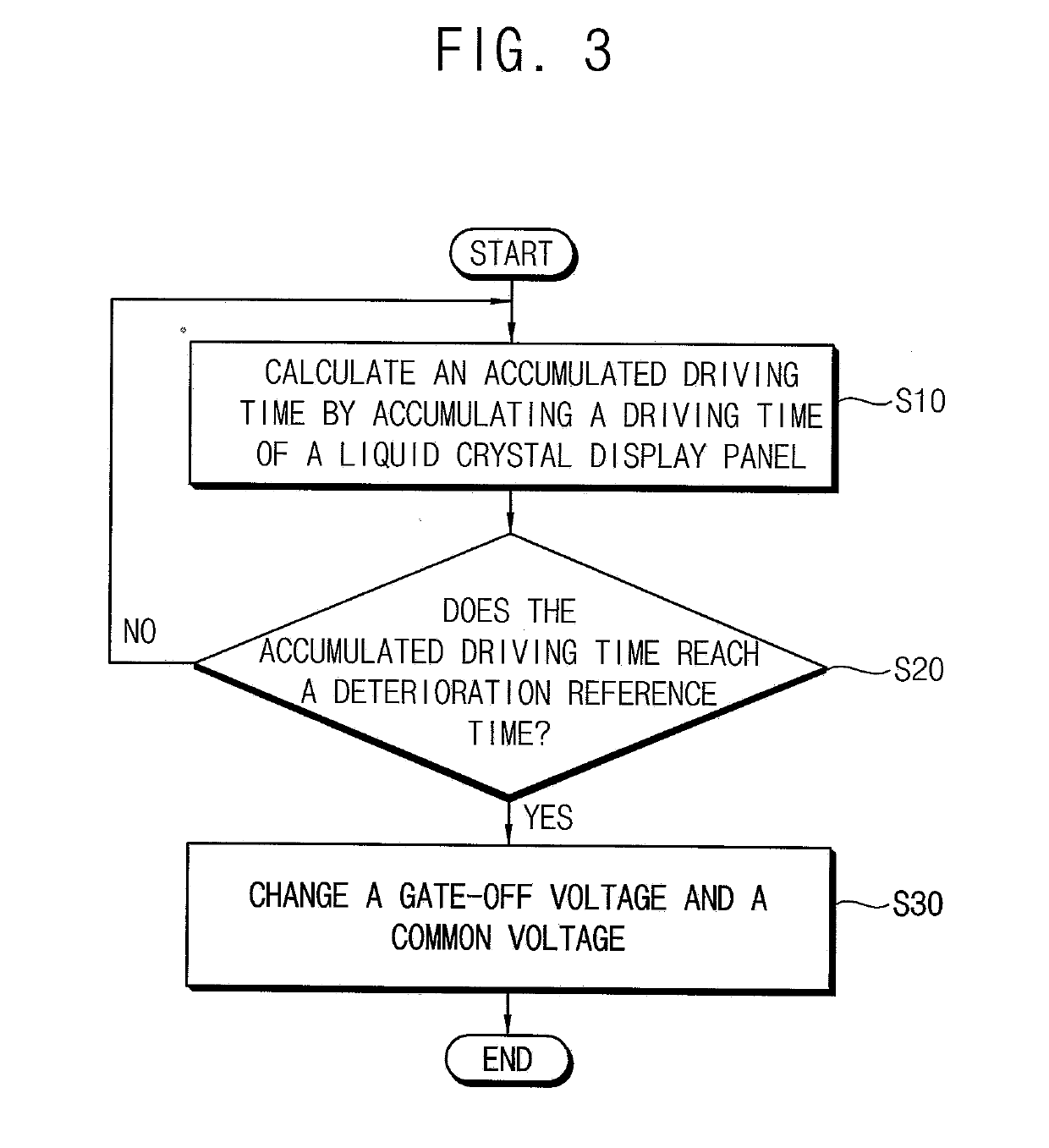
The present invention provides a method and device for driving a liquid crystal display panel that can prevent or mitigate the yellowing phenomenon, which is caused by accumulating a driving time of the display panel. The method calculates the accumulated driving time and changes the gate-off voltage and common voltage when the accumulated driving time reaches a predetermined reference time. This results in a high-quality image even when the liquid crystal display panel deteriorates.

Problems solved by technology

The switching transistor included in the liquid crystal display pixel may deteriorate as an accumulated driving time of the liquid crystal display pixel increases.

Method used


Image

  • Method of driving a liquid crystal display panel and liquid crystal display device employing the same
  • Method of driving a liquid crystal display panel and liquid crystal display device employing the same
  • Method of driving a liquid crystal display panel and liquid crystal display device employing the same

Examples


Embodiment Construction

[0049]Hereinafter, the present invention will be explained in detail with reference to example embodiments shown in the accompanying drawings.

[0050]It will be understood that when an element or layer is referred to as being “on,”“connected to,” or “coupled to” another element or layer, it may be directly on, connected, or coupled to the other element or layer or one or more intervening elements or layers may also be present. When an element or layer is referred to as being “directly on,”“directly connected to,” or “directly coupled to” another element or layer, there are no intervening elements or layers present. For example, when a first element is described as being “coupled” or “connected” to a second element, the first element may be directly coupled or connected to the second element or the first element may be indirectly coupled or connected to the second element via one or more intervening elements.

[0051]The same reference numerals designate the same elements. As used herein,...


PUM

PropertyMeasurementUnit
liquid crystal structureaaaaaaaaaa
structureaaaaaaaaaa
driving timeaaaaaaaaaa

Abstract

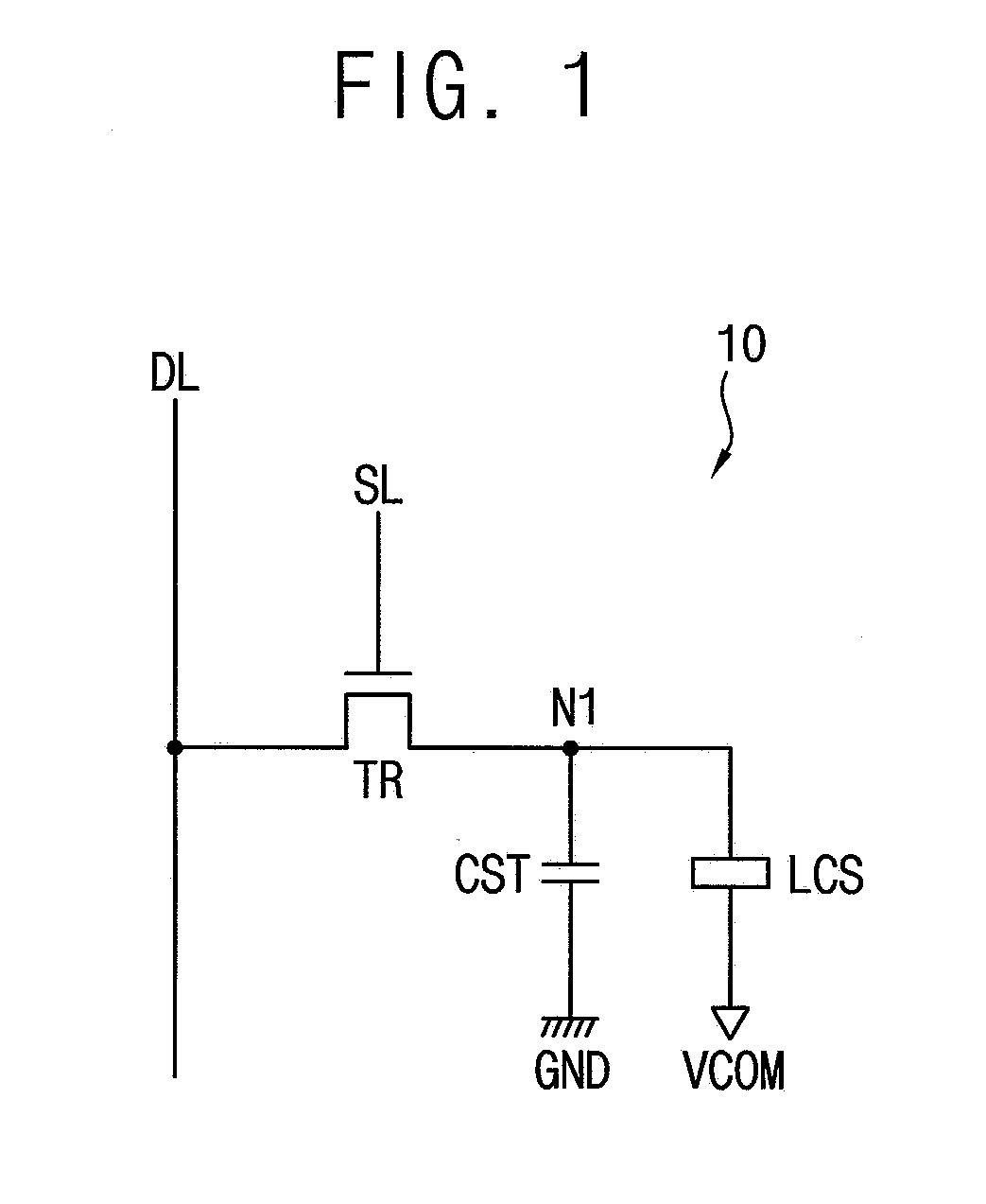
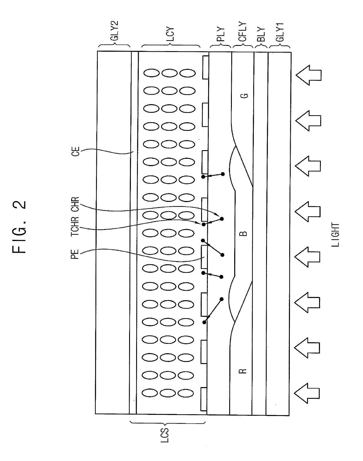
A method of driving a liquid crystal display panel is provided. The liquid crystal display panel includes: a liquid crystal display pixel including a liquid crystal structure including a pixel electrode, a liquid crystal layer, and a common electrode; a switching transistor connected between the pixel electrode of the liquid crystal structure and a data-line; and a storage capacitor connected to the pixel electrode of the liquid crystal structure. The method includes: calculating an accumulated driving time of the liquid crystal display panel by accumulating a driving time of the liquid crystal display panel; determining whether or not the accumulated driving time has reached a deterioration reference time; and when the accumulated driving time is determined to have reached the deterioration reference time, changing a gate-off voltage applied to a gate terminal of the switching transistor and a common voltage applied to the common electrode.

Description

CROSS-REFERENCE TO RELATED APPLICATION[0001]This application claims priority to and the benefit of Korean Patent Application No. 10-2018-0014540, filed on Feb. 6, 2018 in the Korean Intellectual Property Office (KIPO), the entire content of which is incorporated herein by reference.BACKGROUND1. Field[0002]Aspects of example embodiments of the present invention relate generally to a display device.2. Description of the Related Art[0003]Generally, a liquid crystal display device includes a liquid crystal display panel that includes a liquid crystal display pixel, a backlight (e.g., a backlight unit) that provides light to the liquid crystal display panel, a backlight driver (e.g., a backlight unit driving circuit) that drives the backlight, and a liquid crystal display panel driver (e.g., a liquid crystal display panel driving circuit) that drives the liquid crystal display panel. The liquid crystal display pixel includes a switching transistor, a storage capacitor, a liquid crystal s...

Claims


Application Information

Patent Timeline
Patent Type & Authority Applications(United States)
IPC IPC(8): G09G3/36G02F1/1362G02F1/1368G09G3/34
CPCG09G3/3696G02F1/136213G02F1/1368G09G3/3406G09G3/3677G09G3/3688G09G2310/08G09G2320/048G09G2320/045G09G2300/0819G02F2201/121G02F2201/123G09G3/3655G09G3/3648G09G2320/043
Inventor KWON, SANGANLEE, JUNPYOKIM, KYUNHOKIM, SUNGJINSHIN, YONG-JINLEE, NEUNG-BEOMLIM, KYUNG-HWAJANG, JINHYUK
Owner SAMSUNG DISPLAY CO LTD
Learn More