Manufacturing method for semiconductor laminated film, and semiconductor laminated film

a manufacturing method and technology of laminated film, applied in the direction of semiconductor devices, vacuum evaporation coatings, coatings, etc., can solve the problems that the related art has not been able to achieve, and achieve the effects of reducing the mismatch rate of lattice, reducing the mismatch rate, and increasing the compressive strain

Active Publication Date: 2019-08-08
NAT UNIV CORP TOKYO UNIV OF AGRI & TECH +1
View PDF0 Cites 1 Cited by
  • Summary
  • Abstract
  • Description
  • Claims
  • Application Information

AI Technical Summary

Benefits of technology

[0033]In such semiconductor laminate film, a semiconductor layer 20 can have larger compressive strain (i.e., a lower lattice mismatch rate f) even when the semiconductor layer 20 has a high composition ratio x of germanium (see the details described later). Accordingly, in such semiconductor laminate film, the semiconductor layer is better lattice-matched with the silicon substrate even when the semiconductor layer has a high composition ratio of germanium, and a semiconductor device having excellent characteristics can be produced.

Problems solved by technology

12 and the technology described in JP-A-2008-21674 has faced a difficult problem in terms of a technology for controlling formation of a semiconductor laminate film in the course of forming a SiGe layer having a high composition ratio of Ge (ratio of the number of Ge atoms) and large compressive strain, with which significant improvement in characteristics of a semiconductor device (e.g., an increase in carrier mobility, and an increase in speed of the semiconductor device) can be expected.
Thus, a semiconductor laminate film which leads to production of a semiconductor device having such high performance that the related art has not been able to achieve, or significant improvement in characteristics of the device can be produced.

Method used


Image

  • Manufacturing method for semiconductor laminated film, and semiconductor laminated film
  • Manufacturing method for semiconductor laminated film, and semiconductor laminated film
  • Manufacturing method for semiconductor laminated film, and semiconductor laminated film

Examples


experimental examples

3. Experimental Examples

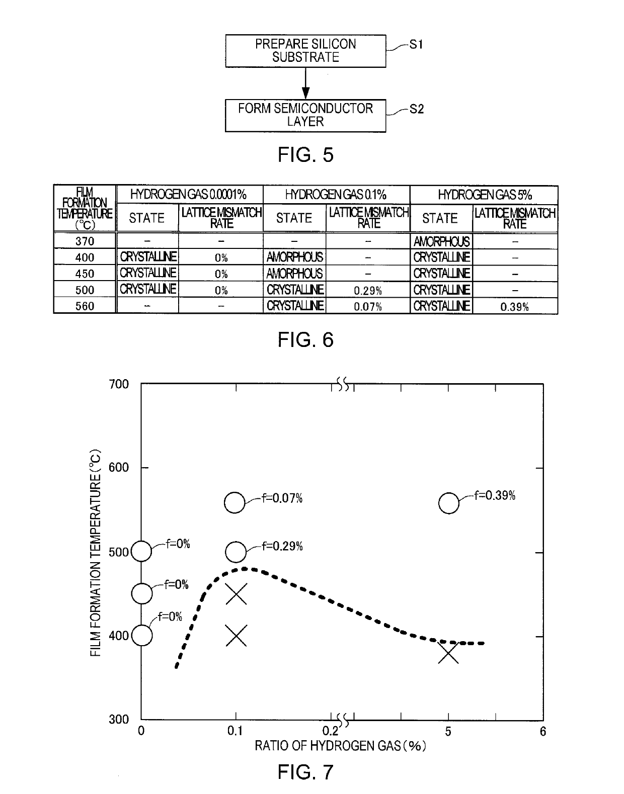
[0094]The invention is described in more detail by way of Experimental Examples below. The invention is by no means limited by the following Experimental Examples.

3.1. Production of Sample

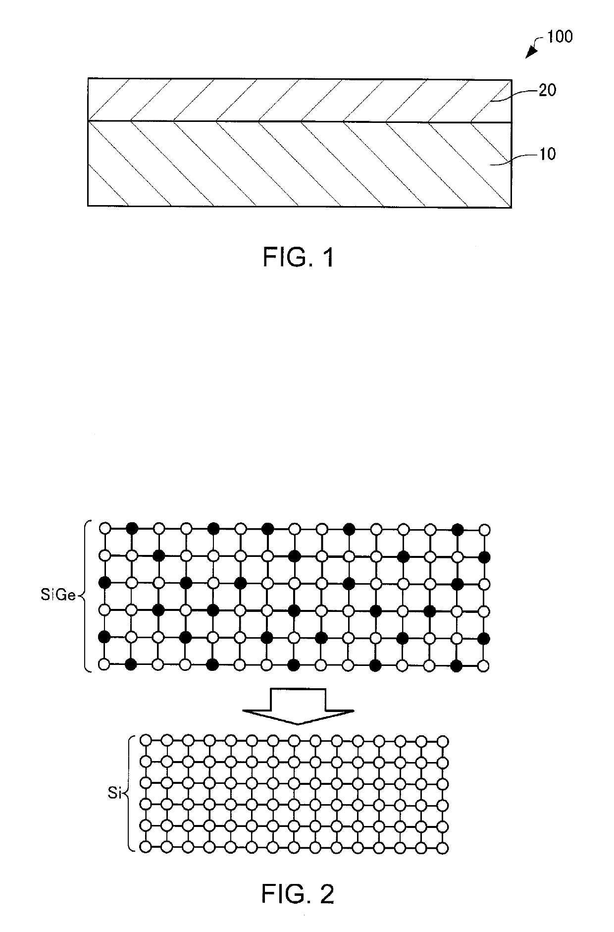
[0095]A SiGe layer was formed on a Si substrate by a sputtering method with a device in which a vacuum reaction vessel (chamber) and a sample introduction vessel (chamber) were connected to each other through a vacuum valve. The vacuum reaction vessel is equipped with a magnetron sputtering gun for Si and a magnetron sputtering gun for Ge.

[0096]Specifically, first, the vacuum reaction vessel was evacuated to vacuum. More specifically, the vacuum valve was closed, and the vacuum reaction vessel was evacuated to 1×10⁻⁹ Torr or less. Moreover, while the vacuum valve was closed, the Si substrate was placed in the sample introduction vessel. Next, the sample introduction vessel was evacuated to a vacuum of 1×10⁻⁷ Torr or less with a turbomolecular pump and a rotary pump each conn...


PUM

PropertyMeasurementUnit
pressureaaaaaaaaaa
temperatureaaaaaaaaaa
formation pressureaaaaaaaaaa

Abstract

A method of producing a semiconductor laminate film includes forming a semiconductor layer containing silicon and germanium on a silicon substrate by a sputtering method. In the sputtering method, a film formation temperature of the semiconductor layer is less than 500° C., and a film formation pressure of the semiconductor layer ranges from 1 mTorr to 11 mTorr, or, a film formation temperature of the semiconductor layer is less than 600° C., and a film formation pressure of the semiconductor layer is equal to or more than 2 mTorr and less than 5 mTorr. The sputtering method uses a sputtering gas having a volume ratio of a hydrogen gas of less than 0.1%, and the semiconductor layer satisfies a relationship of t≤0.881×x−4.79, where t represents a thickness (nm) of the semiconductor layer, and x represents a ratio of the number of germanium atoms to a sum of the number of silicon atoms and the number of germanium atoms in the semiconductor layer.

Description

CROSS REFERENCE TO RELATED APPLICATIONS[0001]This application is a U.S. National Phase application of International Application No. PCT / JP2017 / 025436 filed on Jul. 12, 2017 and published in Japanese as WO 2018 / 012546 A1 on Jan. 18, 2018 and claims the benefit of priority from Japanese Patent Application No. 2016-140117 filed on Jul. 15, 2016. The entire disclosures of all of the above applications are incorporated herein by reference.BACKGROUNDTechnical Field[0002]The present invention relates to a method of producing a semiconductor laminate film, and a semiconductor laminate film.Related Art[0003]As next-generation Si-based ultra-high speed devices, for example, the following devices for communication have been known: high electron mobility transistors (HEMTs); doped-channel field-effect transistors (DCFETs); resonant tunneling diodes (RTDs); hetero-bipolar transistors (HBTs); and strained-channel metal-oxide-semiconductor field-effect transistors (MOSFETs). Of those devices, part...

Claims


Application Information

Patent Timeline
Patent Type & Authority Applications(United States)
IPC IPC(8): C23C14/34C23C14/14H01L21/203H01L29/165H01L29/737H01L29/778H01L29/78H01L29/812H01L29/88
CPCC23C14/34C23C14/14H01L21/203H01L29/165H01L29/737H01L29/778H01L29/78H01L29/812H01L29/88C23C14/06H01L29/161H01L21/02631H01L21/02532H01L21/02381H01L21/02365C23C14/165
Inventor SUDA, YOSHIYUKITSUKAMOTO, TAKAHIROMOTOHASHI, AKIRADEGURA, KYOHEIOKUBO, KATSUMIYAGI, TAKUMAKASAMATSU, AKIFUMIHIROSE, NOBUMITSUMATSUI
Owner NAT UNIV CORP TOKYO UNIV OF AGRI & TECH
Why Eureka
Try Eureka