System and method for enhancing bandwidth of low-dropout regulators using power transmission lines for high speed input output driver
a technology of power transmission lines and regulators, which is applied in the direction of high frequency circuit adaptations, process and machine control, instruments, etc., can solve the problems of excessive power supply noise coupling from input, power supply rejection peaking, power supply noise passing through, etc., to enhance the effective noise-rejection bandwidth of ldo, reduce power supply noise, and increase energy efficiency
- Summary
- Abstract
- Description
- Claims
- Application Information
AI Technical Summary
Benefits of technology
Problems solved by technology
Method used
Image
Examples
case 1
[0050] LDO Dropout Voltage, VDO=0.4V
[0051]In the first study, the dropout voltage across the LDO PMOS transistor was set as 0.4V. For ILOAD=0.1 A, the power absorbed by the PDN is PPDN=I2LOAD*RDC-plane=50 uW; the power loss due to the PMOS transistor is PDO=ILOAD*VDO=40 mW and output power is POUT=ILOAD*VOUT=80 mW. Therefore, the input power is 50 uW+40 mW+80 mW=120.05 mW according to:
PIN=(PPDN+PDO)+POUT=PLOSS+POUT (9)
The energy conversion efficiency of the system is therefore:
ηSYS=POUTPIN=80120.5=66.6%(10)
The LDO power supply noise at node VIN in FIG. 5 can be calculated as:
VINnoise=ZIN*Inoise (11)
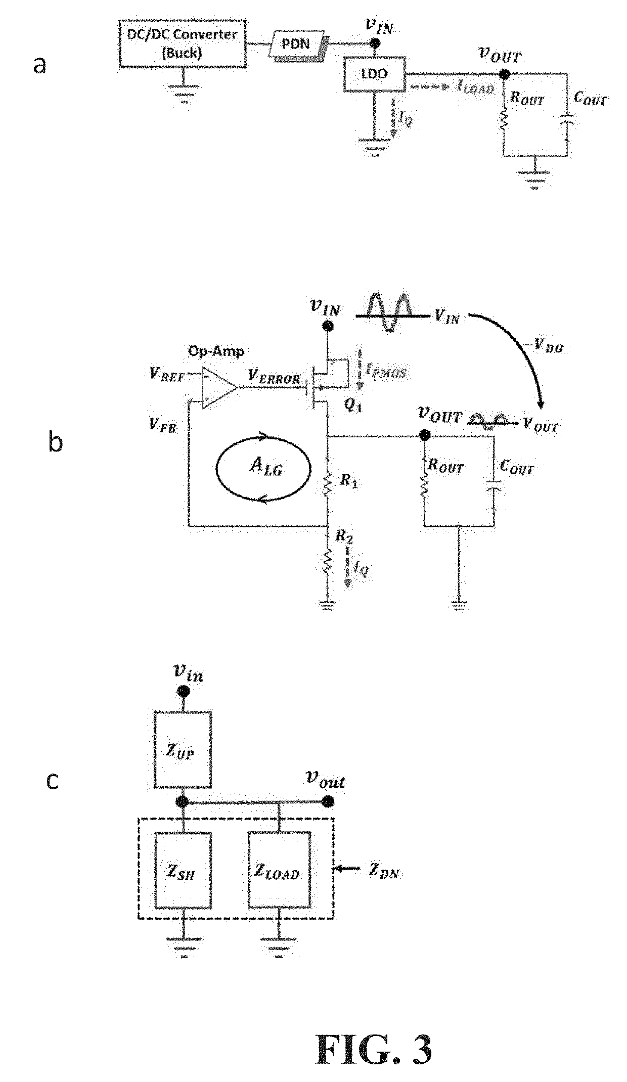
where Inoise is the noise current, which is assumed to be 5 mA, and ZIN is 99.45Ω from the simulation results. Based on the LDO circuit model discussed above, the PSR was calculated as −2.07 dB with a resulting power supply noise at the output of the LDO circuit to be ˜0.39V. The results of this case are shown in Table II below.
case 2
[0052] VDO=0.5V
[0053]In this study, the PSR of the LDO circuit was improved by increasing the dropout voltage to 0.5V. As can be seen in Table II, the PSR improves by 16.6% to −3.65 dB, which was obtained by setting VOUT=0.7V in the simulated LDO model. The resulting power supply noise at the output of the LDO circuit is ˜0.33V, which improved by 16.6% as compared to Case 1. However, due to the increased dropout across the PMOS transistor, the power efficiency reduces by 12.5% to 58.3% as compared to Case 1.
[0054]Hence, it is difficult to achieve high efficiency and low power supply noise at the output of the LDO circuit simultaneously, especially at frequencies where the PDN impedance peaks occur, as illustrated by the results in Table II. Utilizing a single dimension PDN like power transmission lines solves this problem, as described below.
Single Dimension Connector
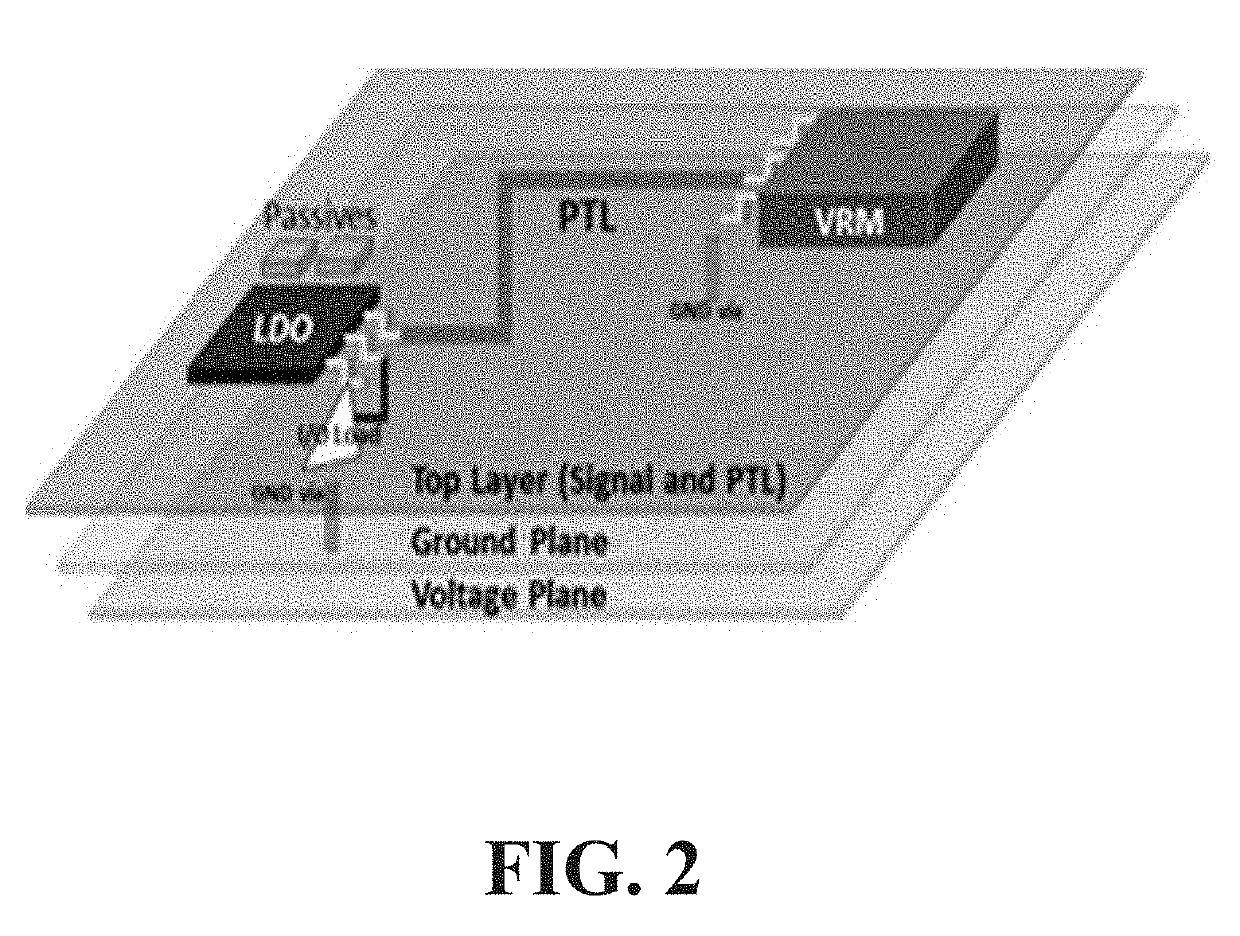
[0055]As shown in FIG. 2, the PDN for the I / O circuits is separated from the core, with the voltage and ground planes...
case 3
[0058] VDO=0.3V
[0059]In FIG. 7, the dropout voltage was set to 0.3V across the PMOS transistor resulting in a worsening of the PSR to −0.405 dB according to the simulated LDO model by setting VOUT=0.9V. However, since the self-impedance of the PDN, which is 1.68Ω, is much lower compared to the previous cases at around 50 MHz, the resulting power supply noise at the output of the LDO circuit is 8.04 mV, as represented by the significantly reduced noise power spike in B3 of FIG. 7 at the LDO out. As compared to Case 1, using a PTL reduces the power supply noise by 97.9%. Though the PTL has a higher simulated DC resistance (48.5 mΩ in this example), the overall energy conversion efficiency is 74.7%, an improvement of 12.1% as compared to Case 1 due to the lower dropout voltage. As can be seen from Table II, the results for Case 3 are much better as compared to both Cases 1 and 2 in terms of efficiency and power supply noise.
[0060]Therefore, co-designing the PTL with the LDO circuit lea...
PUM
 Abstract
Description
Claims
Application Information
 - R&D
- Intellectual Property
- Life Sciences
- Materials
- Tech Scout
- Unparalleled Data Quality
- Higher Quality Content
- 60% Fewer Hallucinations
Browse by: Latest US Patents, China's latest patents, Technical Efficacy Thesaurus, Application Domain, Technology Topic, Popular Technical Reports.
© 2025 PatSnap. All rights reserved.Legal|Privacy policy|Modern Slavery Act Transparency Statement|Sitemap|About US| Contact US: help@patsnap.com


