
SRAM memory with improved end-of-read riggering

a technology of end-of-read rigging and sram memory, which is applied in the field of sram type memories, can solve the problems of increasing access time, generating unnecessary consumption, and reading error of stored data, and achieve the effect of slowing down the variation in potential of said nod

Active Publication Date: 2019-07-25
COMMISSARIAT A LENERGIE ATOMIQUE ET AUX ENERGIES ALTERNATIVES
View PDF4 Cites 0 Cited by
  • Summary
  • Abstract
  • Description
  • Claims
  • Application Information

AI Technical Summary

Benefits of technology

The patent describes a circuit that triggers an end-of-read operation based on a statistical average of the states of all the bit lines. This ensures that the circuit can handle the worst cases of discharging time that meet a specific criterion. The circuit can also be connected to a circuit portion that slows down the variation in potential of the circuit. These features improve the reliability and efficiency of the circuit.

Problems solved by technology

If the sense amplifier is triggered too early, there is a risk of a read error of the stored information but a triggering that is too late leads to increasing the access time and generating unnecessary consumption.
This optimisation is difficult to implement all the more so that for standard SRAM memory devices, generally a high output is sought that can be of 6σ (σ being a standard deviation) and correspond approximately to 2 defective cells out of a billion.
This solution however tends to increase the global space of the memory device.
Moreover, optimising the aforementioned duration T is more arduous for devices that operate on low voltage, or wherein an adjustment in the supply voltage is implemented.

Method used


Image

  • SRAM memory with improved end-of-read riggering
  • SRAM memory with improved end-of-read riggering

Examples


Embodiment Construction

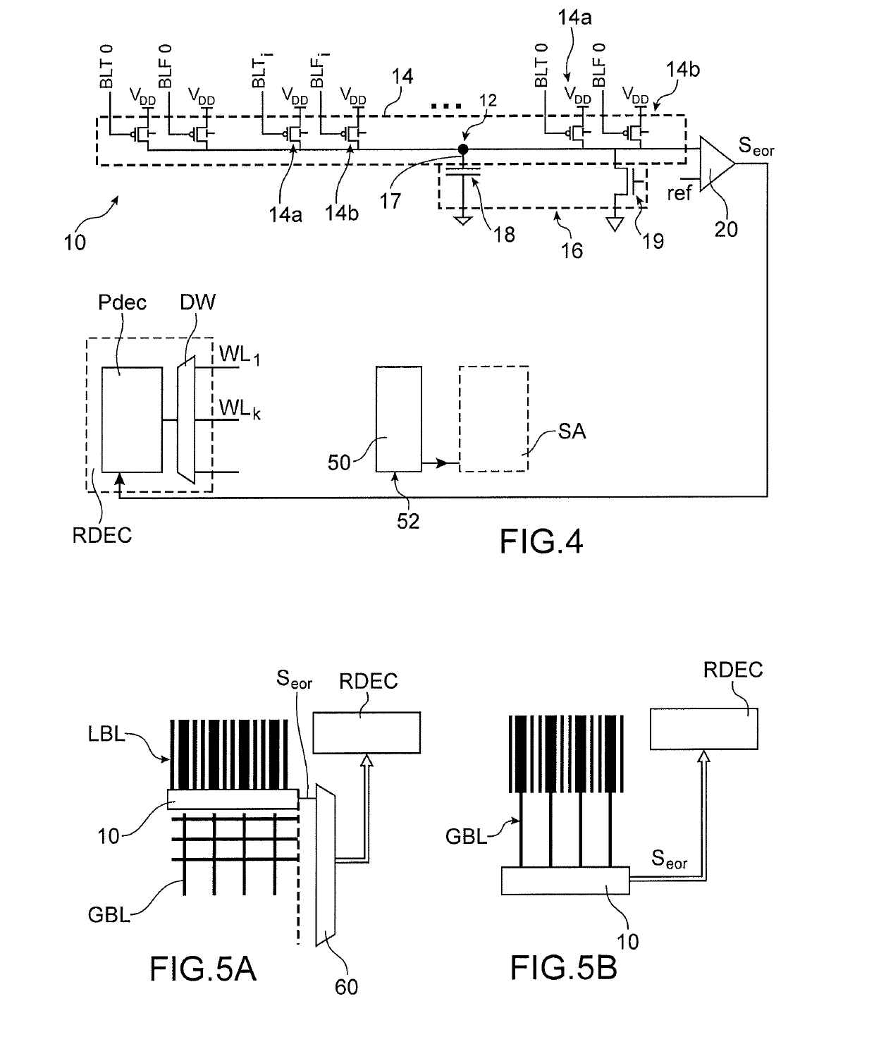
[0049]A circuit for triggering the end of the read operation such as implemented according to the invention is integrated into a SRAM memory device provided with an array plane comprising at least one memory array, for example such as shown in FIG. 2, formed from a plurality of lines and columns of SRAM memory cells.

[0050]The triggering circuit can be implemented without any modification of the internal structure of the SRAM cells C10, . . . Cik, . . . , Cnk and requires the implementation of only a limited number of additional elements peripheral to the memory plane.

[0051]The cells of the memory device can have a conventional arrangement as shown in FIG. 3.

[0052]The cell Cik shown is provided with two storage nodes T and F, provided to store a first piece of logic information, and a piece of logic information complementary to the first piece of information. The maintaining of the logic information in the nodes T, F is provided by transistors that form inverters INV1, INV2 that loop...


PUM


Abstract

Circuit for triggering the end of a read operation, for a SRAM memory device, comprising:a plurality of pairs of transistors connected to a bit line and an additional bit line, the transistors each having a source connected to a node, the node and the bit lines being, prior to the activation of said given word line, respectively pre-charged via the pre-charging means, then, when said word line is activated, at least the bit lines are disconnected from the pre-charging means, in such a way as to modify the conduction state of certain transistors and consequently cause a variation in the potential of said node until reaching a determined threshold potential that triggers the emission of an end-of-phase signal.

Description

TECHNICAL FIELD AND PRIOR ART[0001]This invention relates to the field of SRAM type memories (SRAM for “Static Random Access Memory”), and in particular relates to that of the management of the read operations.[0002]This invention implements a circuit that makes it possible to generate a signal that indicates the end of a particular phase of a read operation and is adapted very particularly to devices that operate on a low voltage or in which a supply voltage scaling is implemented during the various operating phases of the memory.[0003]In SRAM memories, an optimum synchronisation of the various phases of a read operation is particularly important both for providing a high speed and reduced access time while still avoiding read errors, in particular in the presence of time and space variations from one location to another of the memory.[0004]FIG. 1 shows, through the example of a chronogram, a sequence of various phases of a read operation in a conventional SRAM memory. It is assume...

Claims


Application Information

Patent Timeline
Patent Type & Authority Applications(United States)
IPC IPC(8): G11C11/419G11C11/412G11C11/418
CPCG11C11/419G11C11/412G11C11/418G11C7/08
Inventor MAKOSIEJ, ADAMROYER, PABLO
Owner COMMISSARIAT A LENERGIE ATOMIQUE ET AUX ENERGIES ALTERNATIVES
Learn More