Ceramic electronic device

a technology of ceramic electronic devices and ceramic plates, applied in the direction of fixed capacitor details, stacked capacitors, fixed capacitors, etc., can solve problems such as cracks in chip components, and achieve the effects of improving durability, hard to be molten, and improving heat resistan

Active Publication Date: 2019-05-30
TDK CORPARATION
View PDF0 Cites 4 Cited by
  • Summary
  • Abstract
  • Description
  • Claims
  • Application Information

AI Technical Summary

Benefits of technology

The present invention proposes a ceramic electronic device having improved joint reliability and heat resistance during temperature rising. This is achieved by using a connection member containing Sn and Sb, with a smaller gap between the terminal electrode surface and the opposing surface having a higher Sb / Sn content and higher Sb content compared to the first part of the connection member with a larger gap. This results in a stronger connection between the metal terminal and the chip component, even if the connection member is used in small amounts. The ceramic electronic device has a favorable joint strength and heat resistance even if the use amount of the connection member is small. The ceramic electronic device can also prevent manufacturing variations in joint strength and heat resistance by forming a protrusion on the opposing surface. The connection member has an anchor effect that prevents flow during temperature rising, which prevents release of the connection between the metal terminal and the chip component during mounting. The ceramic electronic device can secure a favorable joint strength during a low temperature, non-temperature rising.

Problems solved by technology

When a use amount of connection member is large, however, the chip component may have cracks, and there is a problem with this ceramic electronic device.

Method used


Image

  • Ceramic electronic device
  • Ceramic electronic device
  • Ceramic electronic device

Examples


Embodiment Construction

[0023]Hereinafter, an embodiment of the present invention is described based on the figures.

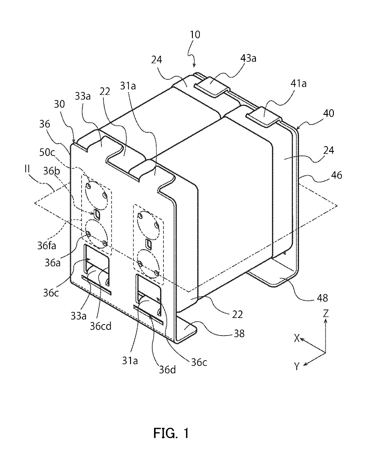
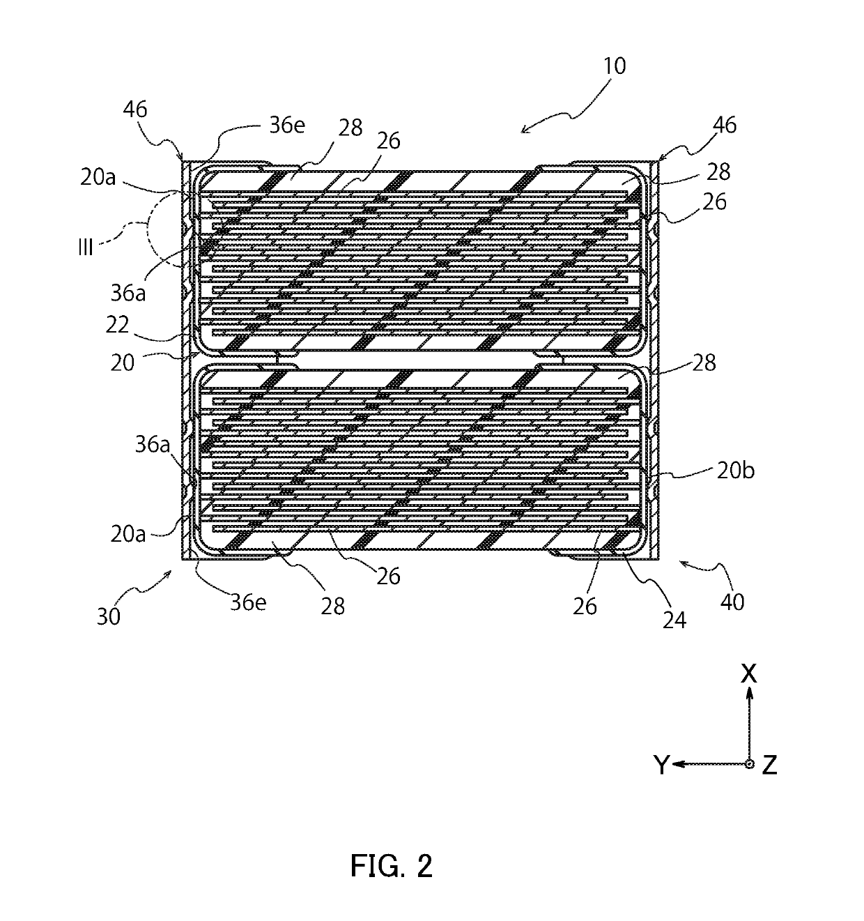
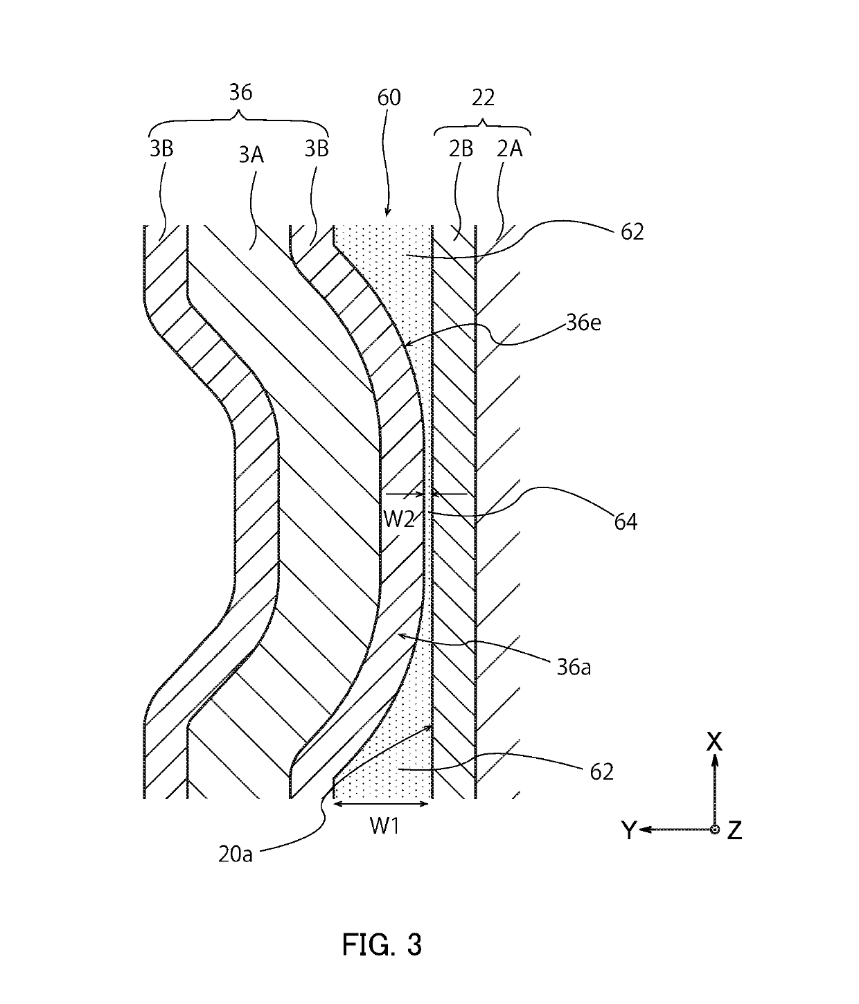
[0024]FIG. 1 is a schematic perspective view illustrating a ceramic capacitor 10 according to an embodiment of the present invention. The ceramic capacitor 10 includes chip capacitors 20 as chip components and a pair of metal terminals 30 and 40. The ceramic capacitor 10 includes two chip capacitors 20, but may include one chip capacitor 20 or three or more chip capacitors 20.

[0025]Incidentally, the embodiment is described with an example of a ceramic capacitor where the metal terminals 30 and 40 are attached to the chip capacitors 20, but the ceramic electronic device of the present invention is not limited to this ceramic capacitor and may be a ceramic electronic device where the metal terminals 30 and 40 are attached to a chip component other than capacitors. As shown in FIG. 1, the embodiment is described with the Z-axis direction vertical to a mount surface, the Y-axis direction parallel...


PUM

PropertyMeasurementUnit
thicknessaaaaaaaaaa
thicknessaaaaaaaaaa
thicknessaaaaaaaaaa

Abstract

A ceramic electronic device includes a chip component, a metal terminal, and a conductive connection member. The component includes a terminal electrode surface on which a terminal electrode is formed. The metal terminal includes an opposing surface to the electrode surface. The connection member contains at least Sn and Sb and connects the terminal electrode surface and the opposing surface. The connection member includes a first part and a second part. In the first part, a distance between the terminal electrode surface and the opposing surface is a first distance, and Sb / Sn is a first value. In the second part, a distance between the terminal electrode surface and the opposing surface is a second distance being smaller than the first distance, and Sb / Sn is a second value being larger than the first value.

Description

BACKGROUND OF THE INVENTION[0001]The present invention relates to a ceramic electronic device with metal terminal including a chip component and a metal terminal attached thereto.[0002]In addition to a normal chip component that is solely directly mounted on a board, a chip component attached with a metal terminal is proposed as a ceramic electronic device, such as a ceramic capacitor. It is reported that the ceramic electronic device attached with a metal terminal after being mounted has a reduction effect on a deformation stress that travels from a board to a chip component and a protection effect on a chip component from impacts or so. Thus, the electronic device attached with a metal terminal is used in a field where durability, reliability, and the like are required.[0003]Patent Document 1: JP2000235932 (A)BRIEF SUMMARY OF INVENTION[0004]As a connection member that connects a chip component and a metal terminal, a connection member containing Sn (tin) and Sb (antimony) is propo...

Claims


Application Information

Patent Timeline
Patent Type & Authority Applications(United States)
IPC IPC(8): H01G4/232H01G4/30H01G4/008H01G4/12
CPCH01G4/2325H01G4/30H01G4/008H01G4/12H01G4/232
Inventor ANDO, NORIHISAMASUDA, SUNAOMORI, MASAHIROMATSUNAGA, KAYOUYAZAWA, KOSUKE
Owner TDK CORPARATION
Why Eureka
Try Eureka