Thin film transistor array substrate and organic light emitting display device having same
- Summary
- Abstract
- Description
- Claims
- Application Information
AI Technical Summary
Benefits of technology
Problems solved by technology
Method used
Image

Examples
first embodiment
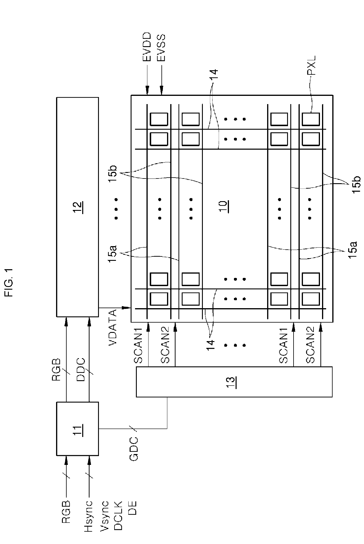
[0050]Next, a thin film transistor array substrate according to the present invention will be explained in more detail by referring to FIGS. 2-5.
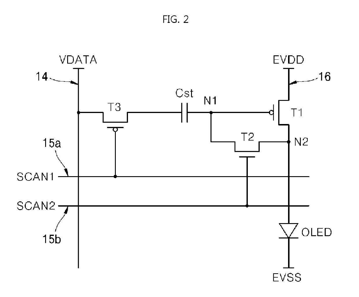
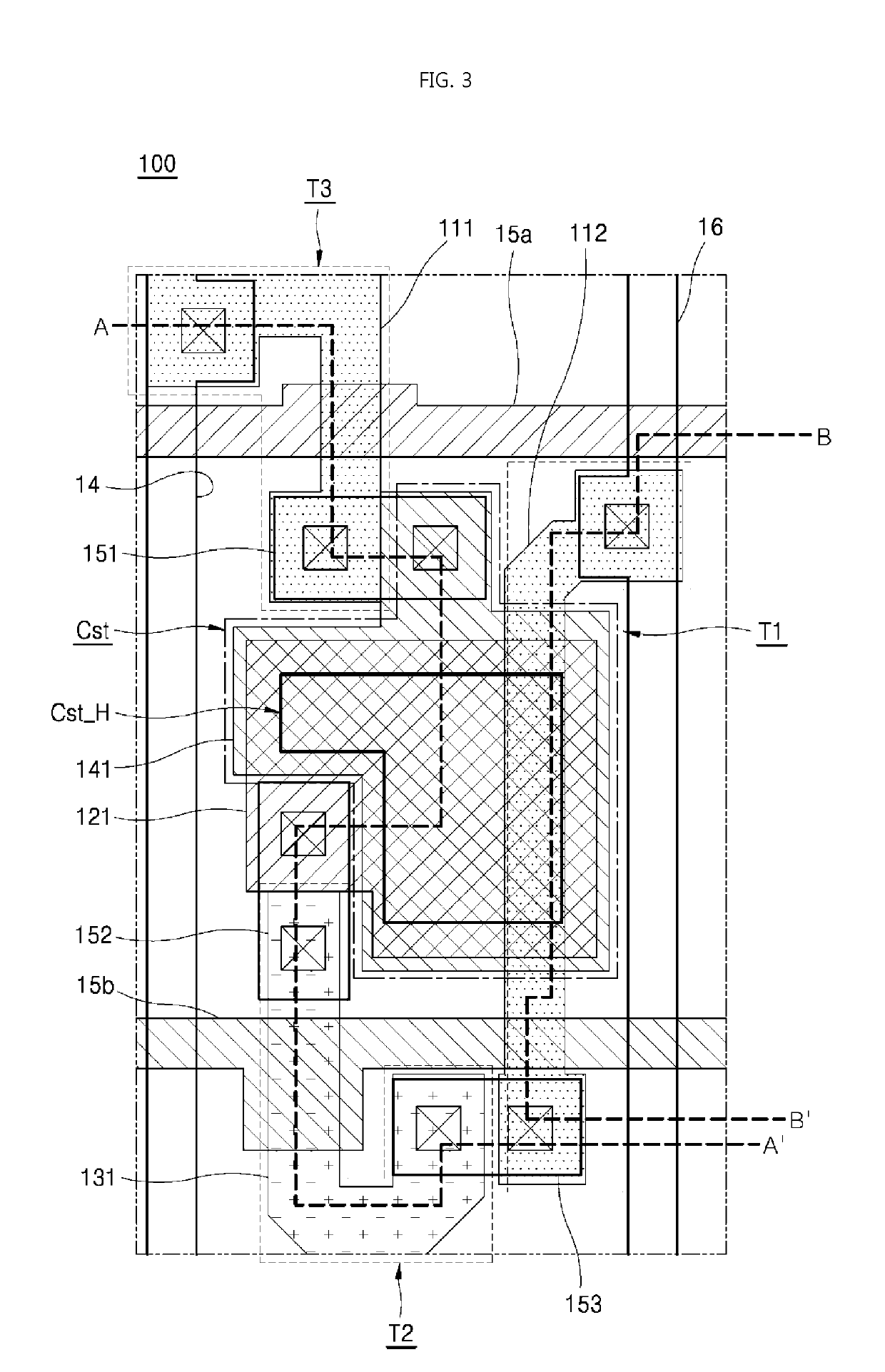
[0051]FIG. 2 is a diagram showing an equivalent circuit corresponding to one pixel in the organic light emitting display device according to the first embodiment of the present invention. FIG. 3 is a diagram shown an example of the thin film transistor array substrate of FIG. 2 having first, second, and third thin film transistors and a capacitor. FIG. 4 is a cross-sectional view taken along a line A-A′ of FIG. 3. FIG. 5 is a cross-sectional view taken along a line B-B′ of FIG. 3.
[0052]As shown in FIG. 2, in the organic light emitting display device according to the first embodiment of the present invention, each of the pixels PXL includes an organic light emitting device OLED, a first thin film transistor T1 for supplying a drive current to the organic light emitting device OLED, a capacitor Cst and a second thin film transistor T2 which a...
second first embodiment
[0097]FIG. 6 is a diagram showing an equivalent circuit corresponding to one pixel in the organic light emitting display device according to the present invention. FIG. 7 is a diagram shown an example of the thin film transistor array substrate of FIG. 6 having first, second, and third thin film transistors and a capacitor. FIG. 8 is a cross-sectional view taken along a line C-C′ of FIG. 7. FIG. 9 is a cross-sectional view taken along a line D-D′ of FIG. 7.
[0098]As shown in FIG. 6, the organic light emitting display device according to the second embodiment of the present invention have the same structure (or substantially the same structure) as the first embodiment shown in FIG. 2 except that the capacitor Cst corresponding to respective pixels PXL is connected between the first and second nodes N1, N2, and that the second thin film transistor T2 is connected between the third node N3, between the first source line 16 and the first thin film transistor T1, and the first node N1. Th...
second embodiment
[0099]More particularly, one of a source electrode and a drain electrode of the first thin film transistor T1 is connected with the first source line supplying the first driving source EVDD while the other one is connected with an anode electrode of the organic light emitting device OLED. Further, a cathode electrode of the organic light emitting device OLED is connected with a second source line supplying a second driving source EVSS.
[0100]The capacitor Cst is connected between one of the source electrode and the drain electrode of the first thin film transistor T1, which is connected with the organic light emitting device OLED, and the gate electrode of the first thin film transistor T1. For example, one of the first and second capacitor electrodes of the capacitor Cst is connected with the first node N1 between the gate electrode of the first thin film transistor T1 and the third thin film transistor T3, while the other one is connected with the second node N2 between the first ...
PUM
 Abstract
Description
Claims
Application Information
 - R&D
- Intellectual Property
- Life Sciences
- Materials
- Tech Scout
- Unparalleled Data Quality
- Higher Quality Content
- 60% Fewer Hallucinations
Browse by: Latest US Patents, China's latest patents, Technical Efficacy Thesaurus, Application Domain, Technology Topic, Popular Technical Reports.
© 2025 PatSnap. All rights reserved.Legal|Privacy policy|Modern Slavery Act Transparency Statement|Sitemap|About US| Contact US: help@patsnap.com