Eureka AIR delivers breakthrough ideas for toughest innovation challenges, trusted by R&D personnel around the world.

Method of manufacturing semiconductor module and semiconductor module

a manufacturing method and technology of semiconductor modules, applied in semiconductor devices, semiconductor/solid-state device details, electrical devices, etc., can solve the problems of poor heat dissipation from the chip mounting portion to the outside of the sealing body

Active Publication Date: 2019-01-03
RENESAS ELECTRONICS CORP
View PDF0 Cites 7 Cited by
  • Summary
  • Abstract
  • Description
  • Claims
  • Application Information

AI Technical Summary

Benefits of technology

The patent aims to improve the reliability of a semiconductor module.

Problems solved by technology

In a power type semiconductor module, in a full mold type structure having a chip mounting portion on which the semiconductor chip is mounted is not exposed from a sealing body, heat dissipation from the chip mounting portion to the outside of the sealing body is poor.

Method used


Image

  • Method of manufacturing semiconductor module and semiconductor module
  • Method of manufacturing semiconductor module and semiconductor module
  • Method of manufacturing semiconductor module and semiconductor module

Examples


first embodiment

[0077]Structure of Semiconductor Module

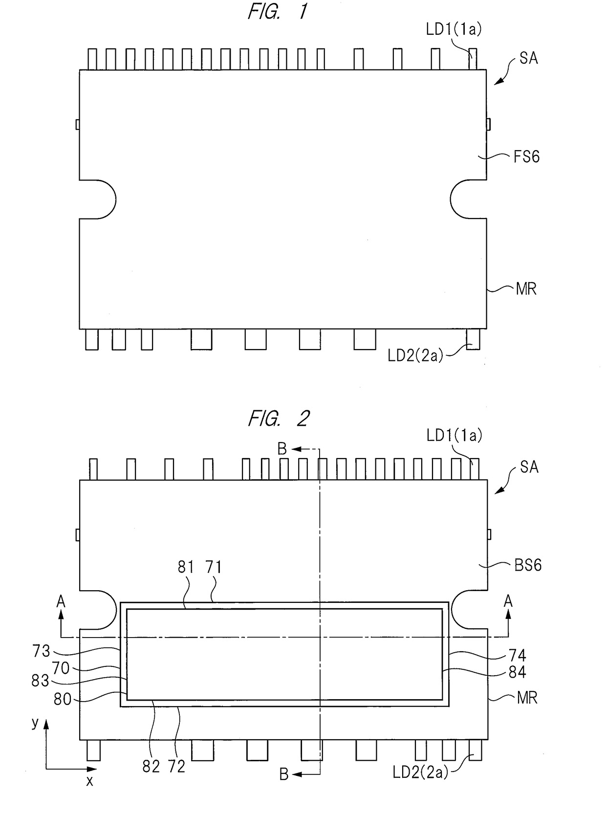
[0078]FIG. 1 is a plan view showing a structure of a semiconductor module of the first embodiment, FIG. 2 is a back view showing the structure of the semiconductor module of FIG. 1, FIG. 3 is a cross-sectional view showing a structure taken along a line A-A of FIG. 2, FIG. 4 is a cross-sectional view showing a structure taken along a line B-B of FIG. 2, and FIG. 5 is a transparent plan view showing an internal structure of the semiconductor module of FIG. 1.

[0079]The semiconductor module according to the first embodiment shown in FIG. 1 to FIG. 5 is used in, for example, a driving circuit of a three-phase induction motor used for an air conditioner or others. More specifically, the drive circuit includes an inverter circuit, and this inverter circuit is a circuit having a function of converting a direct-current power into an alternate-current power.

[0080]The present first embodiment will explain a case of the IGBT as the power transistor embedd...

second embodiment

[0231]FIG. 55 is a back view showing an exposed structure of a chip mounting portion in a structure on a back side of a semiconductor module according to the present second embodiment, and FIG. 56 is a back view showing a structure on the back side of the semiconductor module of the present second embodiment.

[0232]As shown in FIG. 55, on the semiconductor module SA, a control chip 30 for controlling the IGBT chip 10 is mounted. At this time, the control chip 30 tends to be influenced by heat since the control chip is mounted near the heating body such as the IGBT chip 10. Therefore, as shown in FIG. 56, the insulating layer 70 and the TIM layer 80 are bonded in the intended regions so that the insulating layer 70 covers a region W1 of all the chip mounting portions TAB1 to TABS including the chip mounting portion TABS used for the control chip 30 and so that the TIM layer 80 covers a region W2 of all the semiconductor chips. As a result, in the structure shown in FIG. 56, the contro...


PUM


Abstract

Reliability of a semiconductor module is improved. In a resin mold step of assembly of a semiconductor module, an IGBT chip, a diode chip, a control chip, a part of each of chip mounting portions are resin molded so that a back surface of each of the chip mounting portions is exposed from a back surface of a sealing body. After the resin molding, an insulating layer is bonded to the back surface of the sealing body so as to cover each back surface (exposed portion) of the chip mounting portions, and then, a TIM layer is bonded to an insulating layer. Here, a region of the TIM layer in a plan view is included in a region of the insulating layer.

Description

CROSS-REFERENCE TO RELATED APPLICATION[0001]The present application claims priority from Japanese Patent Application No. 2017-128640 filed on Jun. 30, 2017, the content of which is hereby incorporated by reference into this application.TECHNICAL FIELD OF THE INVENTION[0002]The present invention relates to, for example, a method of manufacturing a power semiconductor module (Intelligent Power Module (IPM), electronic device, etc.) and a structure of the power semiconductor module.BACKGROUND OF THE INVENTION[0003]Japanese Patent Application Laid-Open Publication No. 2012-195492 (Patent Document 1) describes a technique relating to a power semiconductor module having a Metal Oxide Semiconductor Field Effect Transistor (MOSFET) and its mounting structure. This power semiconductor module includes a first metal substrate with a power semiconductor element mounted thereon and a second metal substrate without a power semiconductor element mounted thereon, and has such a structure that a bac...

Claims


Application Information

Patent Timeline
Patent Type & Authority Applications(United States)
IPC IPC(8): H01L23/31H01L21/56H01L23/495H01L25/16H01L25/00H01L21/48H01L23/40H01L23/00
CPCH01L23/49537H01L21/565H01L25/165H01L25/50H01L25/162H01L23/4952H01L23/49568H01L21/4842H01L23/4006H01L24/73H01L24/48H01L24/45H01L21/481H01L2224/45144H01L2224/45124H01L2224/49505H01L23/296H01L2224/48101H01L2224/48108H01L2224/48137H01L2224/49112H01L2224/4903H01L2224/48175H01L2924/13055H01L2924/13091H01L2924/1203H01L2224/73265H01L2023/4031H01L2023/405H01L2023/4068H01L2023/4087H01L23/3135H01L23/49562H01L21/56H01L23/36H01L2924/181H01L2224/0603H01L2224/48139H01L2224/48247H01L2224/49171H01L2224/92247H01L23/49541H01L23/49575H01L23/49582H01L23/3107H01L25/072H01L25/18H01L2224/49109H01L24/49H01L2224/32245H01L2224/48096H01L2924/00012H01L2924/00014H01L2924/00
Inventor MUTO, KUNIHARUBANDO, KOJI
Owner RENESAS ELECTRONICS CORP
Why Eureka
Eureka Blog
Learn More