Multilayer substrate and method for manufacturing the same
a technology of multi-layer substrates and manufacturing methods, applied in the direction of dielectric characteristics, printed circuit non-printed electric components association, semiconductor/solid-state device details, etc., can solve the problems of difficult to determine whether the short circuit occurs, and electrical short circuits, and achieve the effect of accurate detection
- Summary
- Abstract
- Description
- Claims
- Application Information
AI Technical Summary
Benefits of technology
Problems solved by technology
Method used
Image

Examples
first preferred embodiment
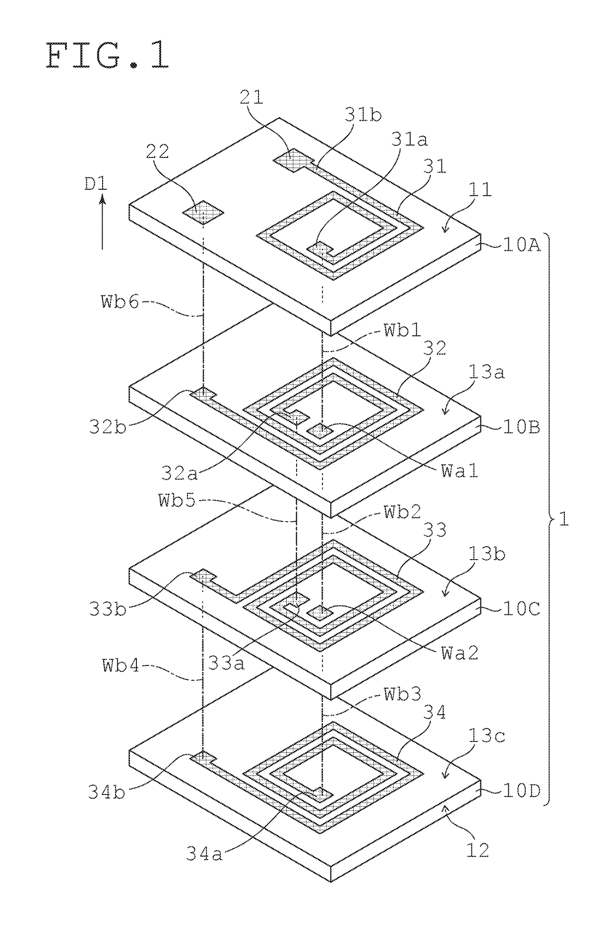
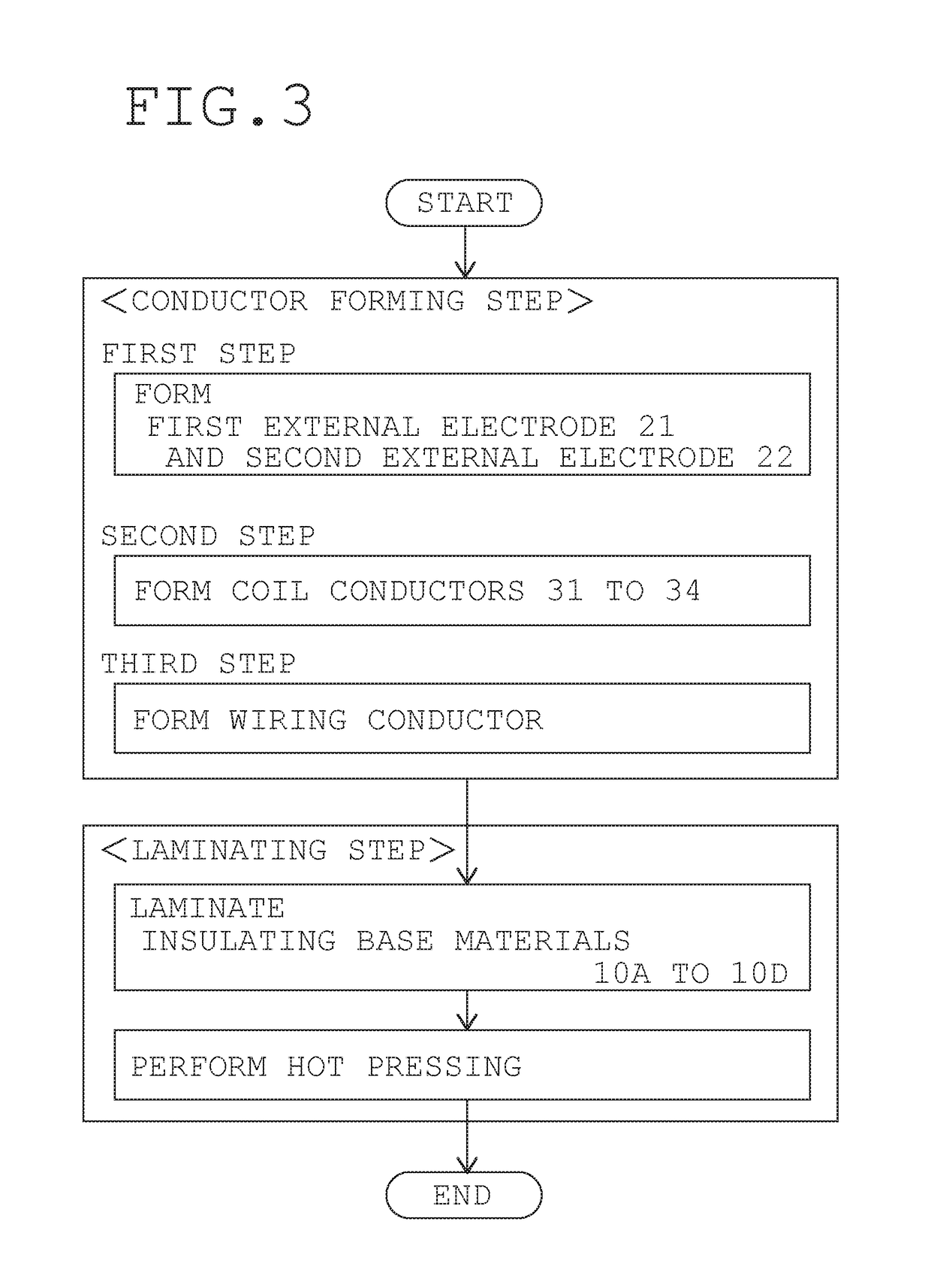
[0036]FIG. 1 is an exploded perspective view conceptually illustrating a multilayer substrate according to a first preferred embodiment of the present invention. As illustrated in FIG. 1, the multilayer substrate includes a laminated body 1, a first external electrode 21, a second external electrode 22, four coil conductors 31 to 34, and a wiring conductor.
[0037]As illustrated in FIG. 1, the laminated body 1 includes four insulating base materials 10A to 10D having thermoplasticity that are laminated together. In the present preferred embodiment, preferably, each of the insulating base materials 10A to 10D, which is made of a thermoplastic resin such as a liquid crystal polymer or a thermoplastic polyimide, for example, has a rectangular or substantially rectangular shape, and has the same or substantially the same size. The laminated body 1 includes a first main surface 11 and a second main surface 12, which are located on opposite sides to each other in a lamination direction D1 o...
second preferred embodiment
[0074]FIG. 5 is an exploded perspective view conceptually illustrating a multilayer substrate according to a second preferred embodiment of the present invention. As illustrated in FIG. 5, in the laminated body 1, the insulating base material 10A may preferably be larger than other insulating base materials 10B to 10D in thickness in the lamination direction D1.
[0075]The following two regions included in the laminated body 1 are considered in this configuration. That is, a first region is defined by a distance X1 from the first main surface 11 in the lamination direction D1 to the laminated interface (in this case, the laminated interface 13a) where the coil conductor (in this case, the coil conductor 32) that is second from the side of the first main surface 11 is provided. A second region is defined by a distance X2 from the second main surface 12 in the lamination direction D1 to the laminated interface (in this case, the laminated interface 13b) where the coil conductor (in this...
third preferred embodiment
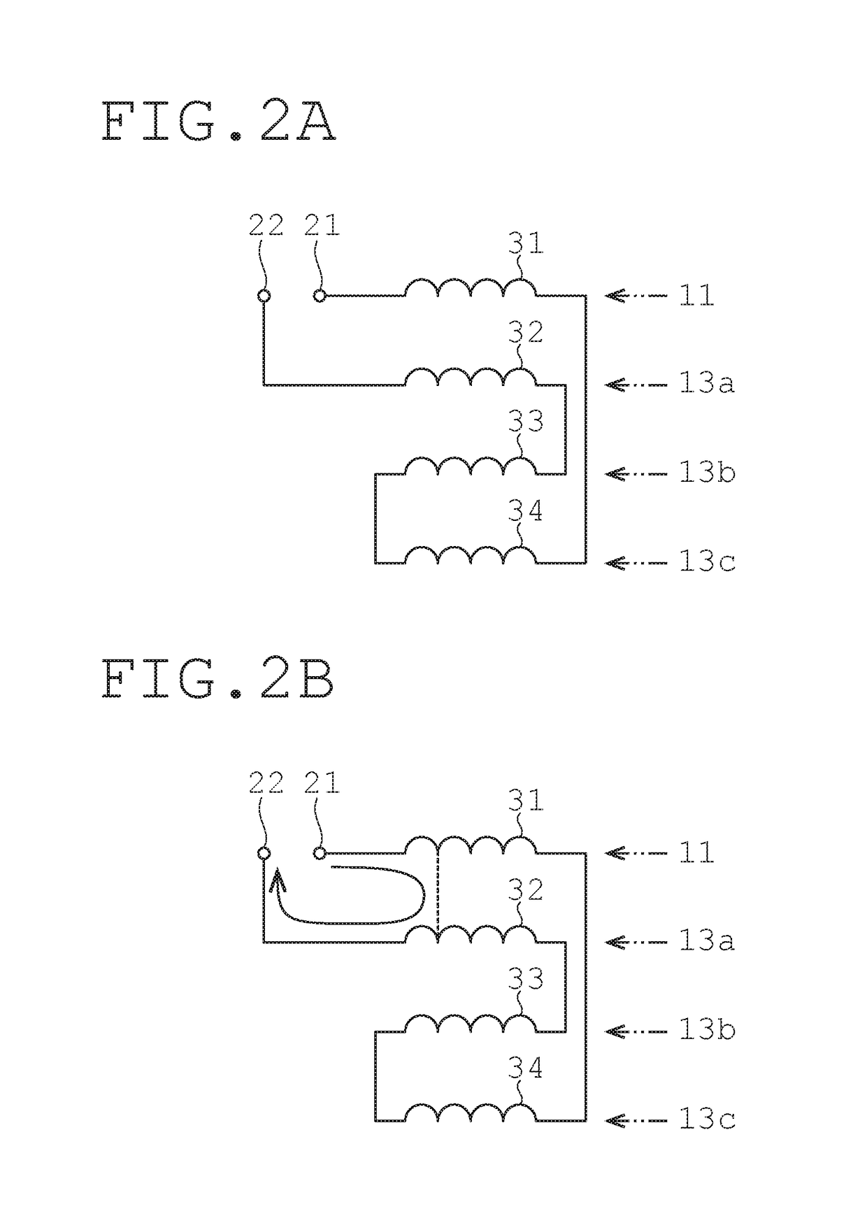
[0092]In the first preferred embodiment, as illustrated in FIGS. 1 and 2A, the coil conductor 31 being the first one from the side of the first main surface 11 is directly connected to the first external electrode 21 as the first coil conductor without other coil conductors interposed therebetween. In addition, the coil conductor 32 being the second one from the side of the first main surface 11 is directly connected to the second external electrode 22 as the second coil conductor without other coil conductors interposed therebetween.
[0093]In the second preferred embodiment, as illustrated in FIGS. 5 and 6A, the coil conductor 34 being the first one from the side of the second main surface 12 is directly connected to the second external electrode 22 as the second coil conductor without other coil conductors interposed therebetween. The coil conductor 33 being the second one from the side of the second main surface 12 is directly connected to the first external electrode 21 as the fi...
PUM
| Property | Measurement | Unit |
|---|---|---|
| thermoplasticity | aaaaa | aaaaa |
| distance | aaaaa | aaaaa |
| size | aaaaa | aaaaa |
Abstract
Description
Claims
Application Information
 - R&D
- Intellectual Property
- Life Sciences
- Materials
- Tech Scout
- Unparalleled Data Quality
- Higher Quality Content
- 60% Fewer Hallucinations
Browse by: Latest US Patents, China's latest patents, Technical Efficacy Thesaurus, Application Domain, Technology Topic, Popular Technical Reports.
© 2025 PatSnap. All rights reserved.Legal|Privacy policy|Modern Slavery Act Transparency Statement|Sitemap|About US| Contact US: help@patsnap.com