
Circuit Board and Electronic Module with an Electrode Structure

a technology of electronic modules and circuit boards, applied in the direction of printed circuits, printed circuit parts, printed circuit non-printed electric components association, etc., can solve the problems of difficulty in viewing the soldering structure between the bottom surface of the conventional electronic module and the corresponding pads on the top surface of the mother board, and cannot be sure whether the soldering is complete between the two boards

Active Publication Date: 2018-11-08
CYNTEC
View PDF14 Cites 1 Cited by
  • Summary
  • Abstract
  • Description
  • Claims
  • Application Information

AI Technical Summary

Benefits of technology

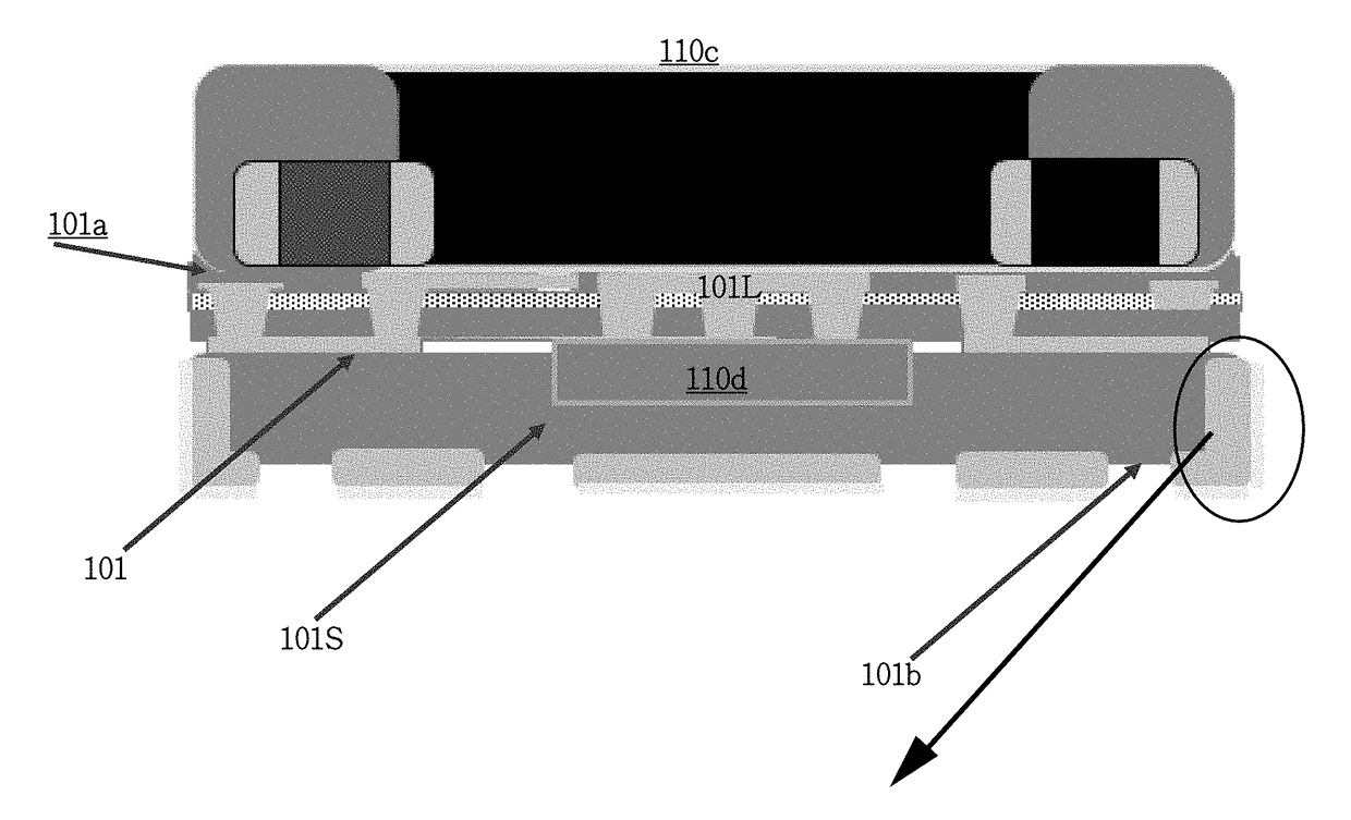
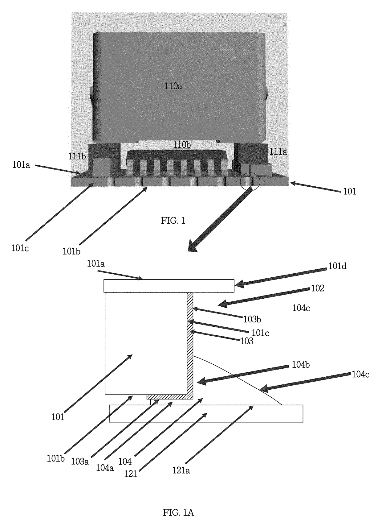
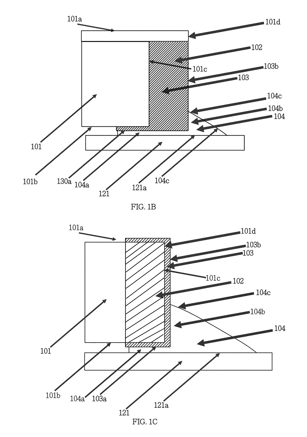
The present invention relates to a circuit board that has a wettable flank, which allows soldering material to be extended to a location outside the circuit board for easier visual checking of the soldering process. Additionally, the soldering material can be extended through the side wall tinning effect, which increases the reliability and strength of the soldering structure between different circuit boards, especially for applications used for vehicles.

Problems solved by technology

When a conventional electronic module needs to connect with a mother board, a soldering material is used to connect the pads on the bottom surface of the conventional electronic module with the corresponding pads on the top surface of the mother board, but it is difficult to view the soldering structure between the bottom surface of the conventional electronic module and the corresponding pads on the top surface of the mother board.
As a result, one cannot be sure whether the soldering is complete between said two boards.

Method used


Image

  • Circuit Board and Electronic Module with an Electrode Structure
  • Circuit Board and Electronic Module with an Electrode Structure
  • Circuit Board and Electronic Module with an Electrode Structure

Examples


Embodiment Construction

[0041]The detailed explanation of the present invention is described as following. The described preferred embodiments are presented for purposes of illustrations and description and they are not intended to limit the scope of the present invention.

[0042]In one embodiment of the present invention, an electronic module is disclosed, wherein the electronic module comprises: a first circuit board, having a top surface, a bottom surface, and a lateral surface connecting the top surface to the bottom surface of the first circuit board; and at least one first electronic device, disposed over the top surface of the first circuit board; and at least one first electronic device, disposed over the top surface of the first circuit board; wherein an electrode structure is disposed on the first circuit board for electrically connecting with an external circuit, wherein the electrode structure 103 comprises a bottom surface and a side surface which acts as a wettable flank on which a soldering ma...


PUM


Abstract

An electronic module is disclosed, wherein the electronic module comprises: a first circuit board, comprising a top surface, a bottom surface, and a lateral surface connecting the top surface and the bottom surface of the first circuit board; wherein an electrode structure is disposed on the first circuit board, wherein a second circuit board is disposed under the bottom surface of the first circuit board, wherein a soldering material is disposed between the bottom surface of the electrode structure and the second circuit board and extended onto a wettable flank of the electrode structure to form a soldering structure, wherein said soldering structure comprises an outer surface that is located above the bottom surface of the first circuit board and outside the outmost portion of the lateral surface of the first circuit board.

Description

CROSS-REFERENCE TO RELATED APPLICATION[0001]This application claims the benefit of U.S. provisional patent application No. 62 / 501,777, filed on May 5, 2017, which is hereby incorporated herein by reference.BACKGROUND OF THE INVENTION1. Field of the Invention[0002]The present invention relates to an electronic module, and more particularly, to an electrode structure of the electronic module for connecting with another circuit board.2. Description of Related Art[0003]When a conventional electronic module needs to connect with a mother board, a soldering material is used to connect the pads on the bottom surface of the conventional electronic module with the corresponding pads on the top surface of the mother board, but it is difficult to view the soldering structure between the bottom surface of the conventional electronic module and the corresponding pads on the top surface of the mother board. As a result, one cannot be sure whether the soldering is complete between said two boards....

Claims


Application Information

Patent Timeline
Patent Type & Authority Applications(United States)
IPC IPC(8): H05K1/11H05K1/18H05K3/42H05K1/09H05K1/14
CPCH05K1/115H05K2201/10378H05K1/185H05K3/423H05K1/09H05K1/14H05K2201/09009H05K2201/1003H05K1/117H05K1/18H05K1/141H05K3/3442H05K3/403H05K2201/09181
Inventor HUANG, CHI-FENG
Owner CYNTEC
Learn More