
Display panel and driving method of display panel

Active Publication Date: 2018-10-18
SAMSUNG ELECTRONICS CO LTD
View PDF2 Cites 49 Cited by
  • Summary
  • Abstract
  • Description
  • Claims
  • Application Information

AI Technical Summary

Benefits of technology

The patent text describes a display panel and a method of driving it that can improve brightness and light emitting efficiency at the same time. This means that the display panel can show the same level of brightness across the entire screen, and it can also produce more light overall.

Problems solved by technology

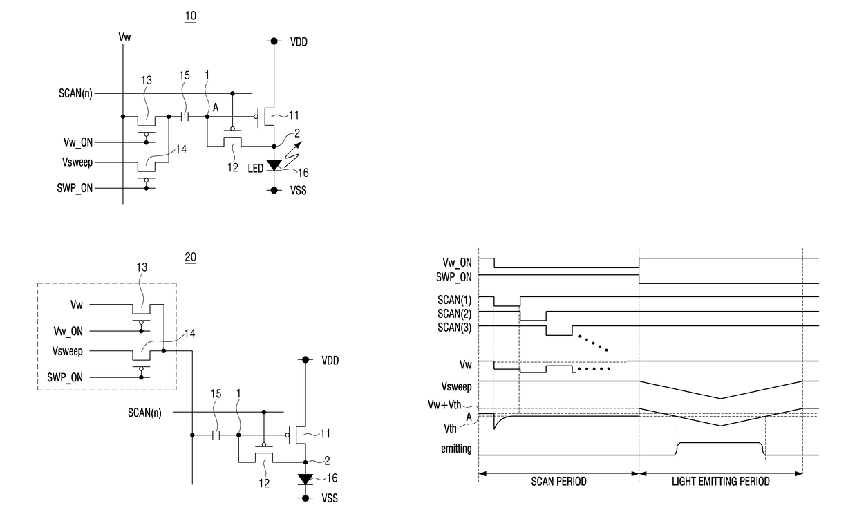
In the case of the digital PWM method, there are problems in that since a TFT (Thin Film Transistor) of a pixel is driven in a linear region, a brightness deviation largely occurs in accordance with a forward voltage (Vf) deviation of an LED and since gradation is represented by a sub-field method, there is a limitation in the number of gradations that may be represented and a false contour occurs.
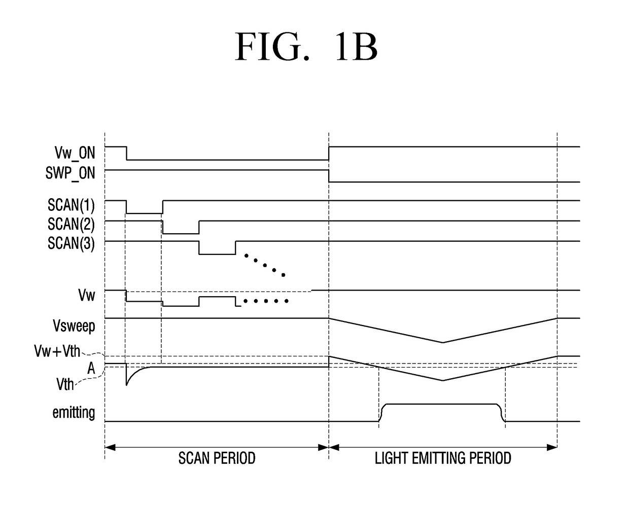
However, in the case of the analog PWM method, brightness uniformity may be problematic due to a deviation of a threshold voltage (Vth) or a mobility deviation (μ) between TFTs (Thin Film Transistors) of each pixel of an LED display panel.
However, since the time used to display one frame is constant (e.g., 1 / 60 second for 60 Hz, and 1 / 120 second for 120 Hz), when the scan time of a line is increased in order to increase a deviation correction effect, an LED emitting duration is reduced, resulting in a problem that the light emitting efficiency is lowered.
Also, when the light emitting duration is increased in order to increase the LED emitting efficiency, an effect of correcting the deviation between TFTs is lowered, resulting in a problem that brightness uniformity deteriorates.
As described above, there is a trade-off relationship between the improvement of the brightness uniformity owing to the improvement of the deviation correction effect and the improvement of the light emitting efficiency in accordance with the increase of the light emitting duration, resulting in a problem that both may not be improved according to the conventional PWM method.

Method used


Image

  • Display panel and driving method of display panel
  • Display panel and driving method of display panel
  • Display panel and driving method of display panel

Examples


Embodiment Construction

[0040]In the description of the disclosure, a detailed description of known related art will be omitted if it is determined that the gist of the disclosure may be unnecessarily obscured. Further, redundant description of the same constitution will be omitted.

[0041]The suffix “unit” for the constituent elements used in the following description is given or mixed only in consideration of easy drafting of the specification, and does not have its own meaning or function to distinguish from each other.

[0042]The terms used in the disclosure are used to illustrate the embodiments and are not intended to limit and / or restrict the disclosure. The singular forms “a,”“an,” and “the” include plural expressions unless the context clearly dictates otherwise.

[0043]In the specification, terms such as “including” or “having” are used to designate the presence of stated features, integers, steps, operations, elements, components, or combinations thereof, but do not preclude the presence or addition o...


PUM


Abstract

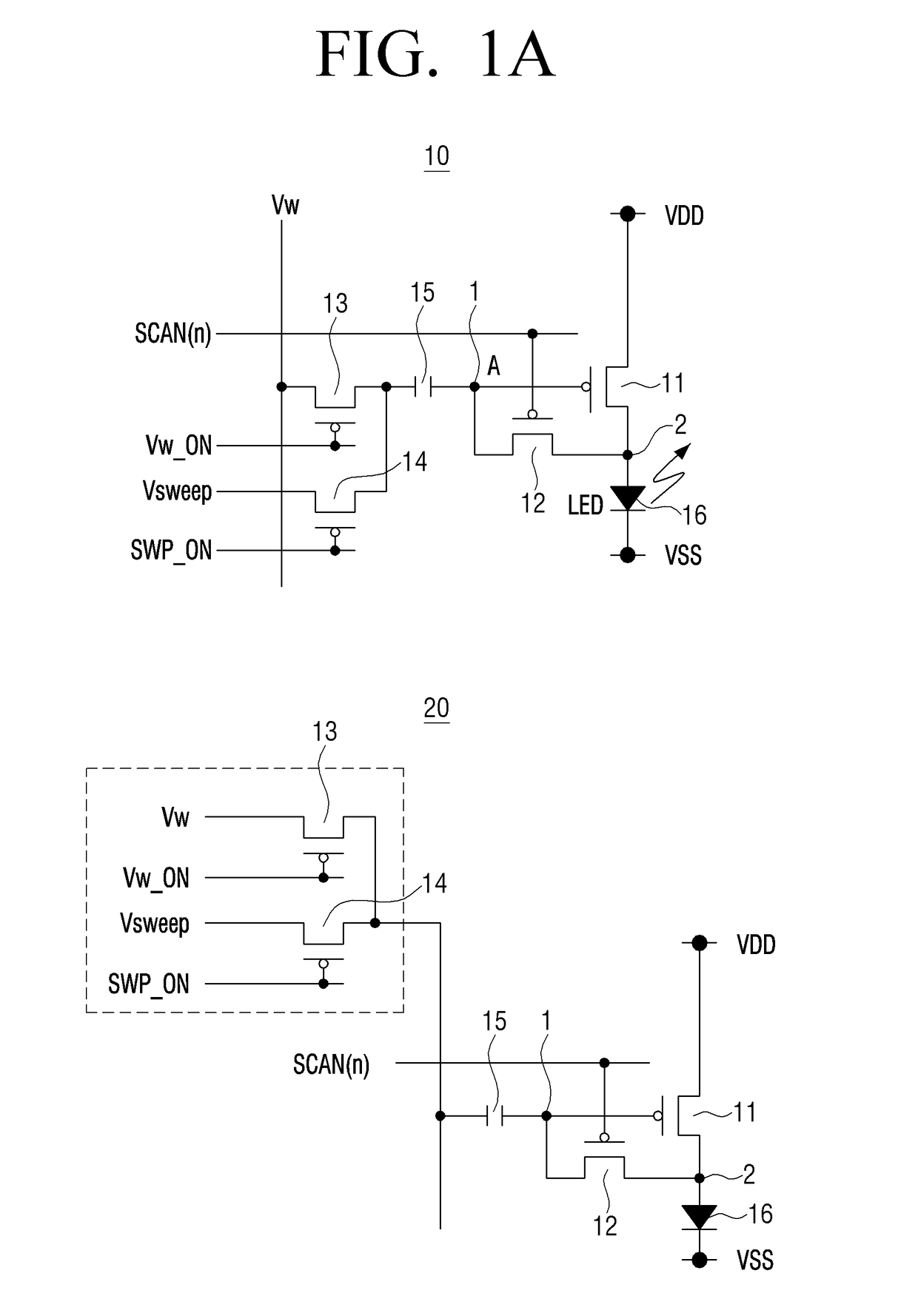
A display panel including a plurality of pixel circuits is provided. Each of the plurality of pixel circuits includes a light emitting unit including a light emitting element; a control circuit configured to control a light emitting duration of the light emitting element based on an input end voltage; a first switching element connected between an input end and an output end of the control circuit; and a signal input unit including a second switching element and configured to transmit an input signal to the input end of the control circuit. The first switching elements of each of the plurality of pixel circuits are configured to simultaneously turn on or off.

Description

CROSS-REFERENCE TO RELATED APPLICATIONS[0001]This application is based on and claims priority under 35 U.S.C. § 119 to Korean Patent Application No. 10-2018-0031625 filed on Mar. 19, 2018 in the Korean Intellectual Property Office, and U.S. Provisional Patent Application No. 62 / 484,971, filed on Apr. 13, 2017 in the United States Patent and Trademark Office, the disclosures of which are incorporated herein by reference in its entirety.BACKGROUNDField[0002]The disclosure relates to a display panel and a driving method of the display panel and, and more particularly, to a display panel driven by an analog PWM (Pulse Width Modulation) method and a driving method of the display panel.Description of the Related Art[0003]A PWM (Pulse Width Modulation) method is widely used as a driving method of an LED (Light Emitting Diode) display panel for representing the gradation of a pixel.[0004]The PWM method includes a digital PWM method and an analog PWM method. In the case of the digital PWM me...

Claims


Application Information

Patent Timeline
IPC IPC(8): G09G3/20G09G3/32
CPCG09G3/2018G09G3/32G09G2310/066G09G2320/0233G09G3/2014G09G3/3208G09G3/3258G09G2300/0819G09G2310/0259
Inventor SHIGETA, TETSUYAPARK, SANG-YOUNGLEE, HO-SEOP
Owner SAMSUNG ELECTRONICS CO LTD
Learn More