Multilayer electronic component

a multi-layer electronic component and electronic component technology, applied in the direction of fixed capacitor details, stacked capacitors, fixed capacitors, etc., can solve the problems of forming gaps between the via-electrode and the ceramic element, and prone to detachment from the ceramic element, so as to reduce the occurrence of cracks, reduce the deformation of the multi-layer electronic component, and easy to form

Active Publication Date: 2018-09-27
MURATA MFG CO LTD
View PDF1 Cites 2 Cited by
  • Summary
  • Abstract
  • Description
  • Claims
  • Application Information

AI Technical Summary

Benefits of technology

The present invention provides methods for making electronic components with multiple layers that are less likely to have breaks or cracks. This is achieved by strengthening the connection between the via-electrode and the ceramic element. The technical effect of this invention is to improve the reliability of multilayer electronic components.

Problems solved by technology

However, if a ceramic element is replaced by the sealing resin layer, the via-electrodes do not linearly contact the ceramic element because of their bellows curved shape.
If the via-electrodes become smaller during the firing process due to the difference in the contraction coefficient, it is likely to detach from the ceramic element.
As a result, gaps may be formed between the via-electrodes and the ceramic element.

Method used


Image

  • Multilayer electronic component
  • Multilayer electronic component
  • Multilayer electronic component

Examples


first preferred embodiment

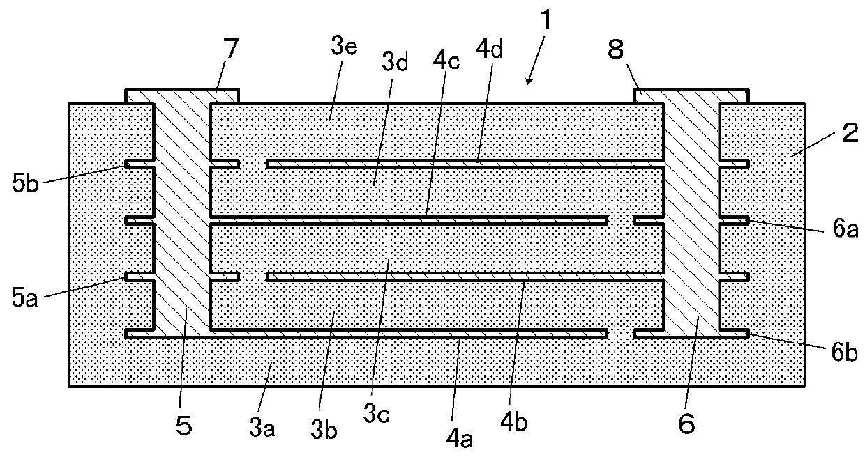
[0030]FIG. 1 illustrates a multilayer electronic component 1 according to a first preferred embodiment of the present invention. The multilayer electronic component 1 will simply be referred to as the electronic component 1. In the first preferred embodiment, a multilayer ceramic capacitor will be described as an example of the electronic component 1. The electronic component 1 includes an electronic component body 2. As shown in FIG. 1, in the electronic component body 2, a plurality of ceramic layers (dielectric layers) 3a through 3e made of a dielectric ceramic material are stacked on each other with a plurality (preferably four in the first preferred embodiment, for example) of inner electrodes 4a through 4d therebetween. The inner electrodes 4a and 4c extend toward the left side of the electronic component body 2 and are connected to a via-electrode 5. The via-electrode 5 is provided at the left side of the electronic component body 2 and passes therethrough in the thickness di...

second preferred embodiment

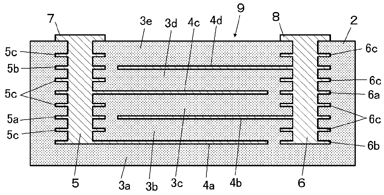
[0047]FIG. 3 illustrates a multilayer electronic component 9 according to a second preferred embodiment of the present invention. The multilayer electronic component 9 will simply be referred to as the electronic component 9. The same elements as those shown in FIG. 1 or elements corresponding to those shown in FIG. 1 are designated by the same reference numerals, and the same explanation will not be repeated.

[0048]In the first preferred embodiment shown in FIG. 1, the projections 5a and 5b of the via-electrode 5 and the projections 6a and 6b of the via-electrode 6 are provided on the same layers, that is, on the same levels, as the corresponding inner electrodes 4a through 4d. In the second preferred embodiment shown in FIG. 3, in addition to the projections 5a, 5b, 6a, and 6b provided on the same layers (on the same levels) as the inner electrodes 4a through 4d, projections 5c and 6c are also provided on different levels from the inner electrodes 4a through 4d. That is, at least o...


PUM

PropertyMeasurementUnit
volume ratioaaaaaaaaaa

Abstract

A multilayer electronic component includes first, second, and third ceramic layers, first and second inner electrodes, and a via-electrode. The first, second and third ceramic layers are sequentially stacked on each other. The first inner electrode is sandwiched between the first and second ceramic layers. The second inner electrode is sandwiched between the second and third ceramic layers. The via-electrode electrically connects the first and second inner electrodes. A projection is integrally provided with the via-electrode. The projection projects from the via-electrode towards an outer peripheral direction and is inserted into the second ceramic layer in a layered arrangement.

Description

CROSS REFERENCE TO RELATED APPLICATIONS[0001]This application claims the benefit of priority to Japanese Patent Application No. 2017-053866 filed on Mar. 21, 2017. The entire contents of this application are hereby incorporated herein by reference.[0002]BACKGROUND OF THE PRESENT INVENTION1. Field of the Present Invention[0003]The present invention relates to a multilayer electronic component. More particularly, the present invention relates to a multilayer electronic component including at least three ceramic layers, at least two inner electrodes sandwiched between the corresponding ceramic layers, and a via-electrode electrically connecting the inner electrodes.2. Description of the Related Art[0004]In a typical multilayer electronic component, via-electrodes (may alternatively be conductive posts or through-holes) are formed to connect a circuit on a certain layer and a circuit formed on a layer above or below this certain layer.[0005]In the multilayer wiring substrate block discl...

Claims


Application Information

Patent Timeline
Patent Type & Authority Applications(United States)
IPC IPC(8): H01G4/232H01G4/012H01G4/008H01G4/30H01G4/242
CPCH01G4/2325H01G4/012H01G4/008H01G4/30H01G4/242H01G4/005H01G4/12H01G4/232
Inventor KAWAKAMI, TETSUOHIRAO, TAKAHIROTANAKA, TSUTOMUKAGEYAMA, TOMOHIRO
Owner MURATA MFG CO LTD
Why Eureka
Try Eureka