Testing transfer-print micro-devices on wafer
- Summary
- Abstract
- Description
- Claims
- Application Information
AI Technical Summary
Benefits of technology
Problems solved by technology
Method used
Image

Examples
Embodiment Construction
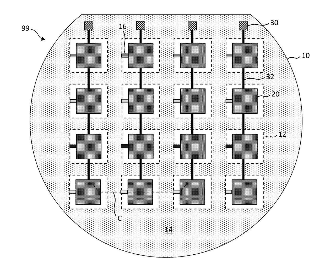
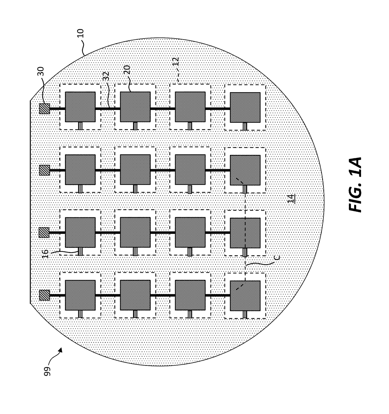
[0040]The present invention provides, inter alia, structures and methods for efficiently and effectively testing transfer printable (e.g., micro-transfer printable) micro-devices on a source wafer. In certain embodiments, defective or faulty micro-devices are removed from the source wafer and the remaining micro-devices are transfer printed (e.g., micro-transfer printed) from the source wafer to a desired destination substrate.
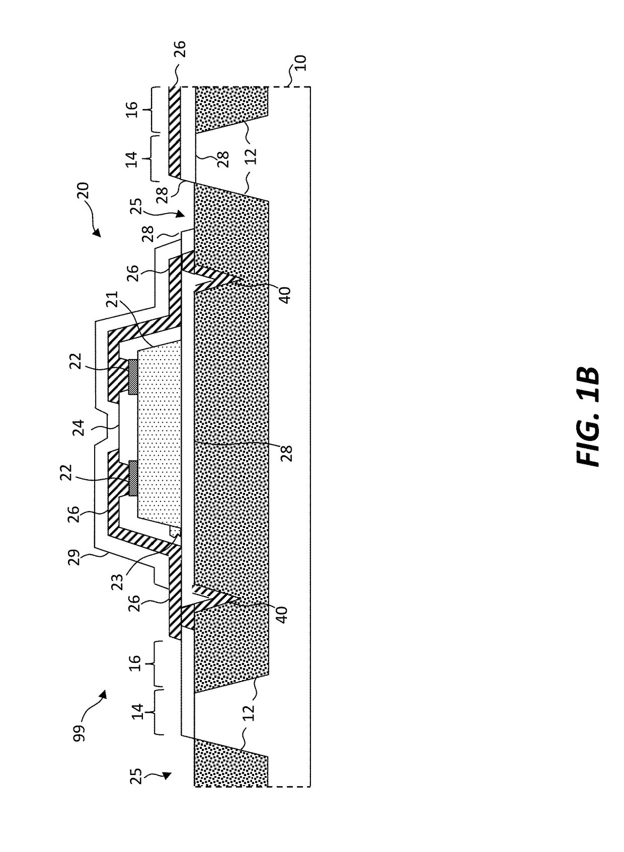
[0041]Certain embodiments of the present invention are illustrated in the plan view of FIG. 1A, the corresponding cross section of FIG. 1B taken across line segment C of FIG. 1A, the alternative detail perspectives of FIGS. 2A and 2B, and the flow diagram of FIG. 3. As shown specifically in FIGS. 1A and 1B, a transfer-printable micro-device wafer system 99 comprises a source wafer 10 having a plurality of sacrificial portions 12 spatially separated by anchors 14. The source wafer 10 has one or more test contact pads 30 that can be electrically connected to ext...
PUM
 Abstract
Description
Claims
Application Information
 - R&D
- Intellectual Property
- Life Sciences
- Materials
- Tech Scout
- Unparalleled Data Quality
- Higher Quality Content
- 60% Fewer Hallucinations
Browse by: Latest US Patents, China's latest patents, Technical Efficacy Thesaurus, Application Domain, Technology Topic, Popular Technical Reports.
© 2025 PatSnap. All rights reserved.Legal|Privacy policy|Modern Slavery Act Transparency Statement|Sitemap|About US| Contact US: help@patsnap.com