
Drain lag compensation circuit for RF power transistors

a technology of drain lag and compensation circuit, which is applied in the field of drain lag compensation circuits for rf (radio frequency) power transistors, can solve the problems of limiting the performance of gallium nitride transistors, reducing drain current, and distortion of output signals, and achieves effective compensation of the drain lag

Inactive Publication Date: 2018-08-23
MACOM TECH SOLUTIONS HLDG INC
View PDF4 Cites 2 Cited by
  • Summary
  • Abstract
  • Description
  • Claims
  • Application Information

AI Technical Summary

Benefits of technology

The patent describes a compensation circuit for reducing the drain lag effect in transistors. The circuit senses the drain voltage and controls the drain current to maintain a constant quiescent drain current through the main transistor. This circuit can be used in a variety of applications, such as RF power amplifiers, and can be fabricated on a single substrate. The technical effect of this patent is to improve the performance and reliability of transistor circuits by reducing the drain lag effect.

Problems solved by technology

A mechanism that limits the performance of gallium nitride transistors is the trapping effect which causes a reduction in drain current after the application of a high voltage.
The effect changes with time and may cause distortion in the output signal.
However, it is difficult to track changes in transistor characteristics using the digital pre-distortion technique.

Method used


Image

  • Drain lag compensation circuit for RF power transistors
  • Drain lag compensation circuit for RF power transistors
  • Drain lag compensation circuit for RF power transistors

Examples


Embodiment Construction

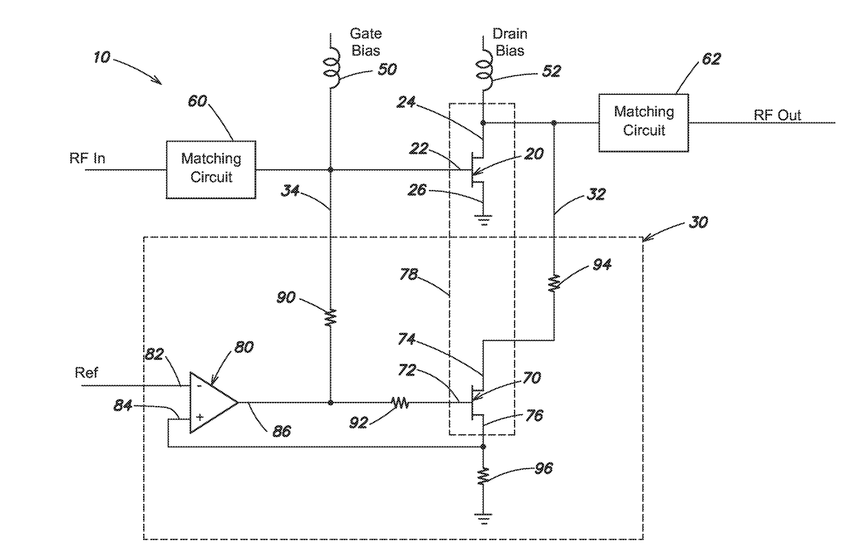
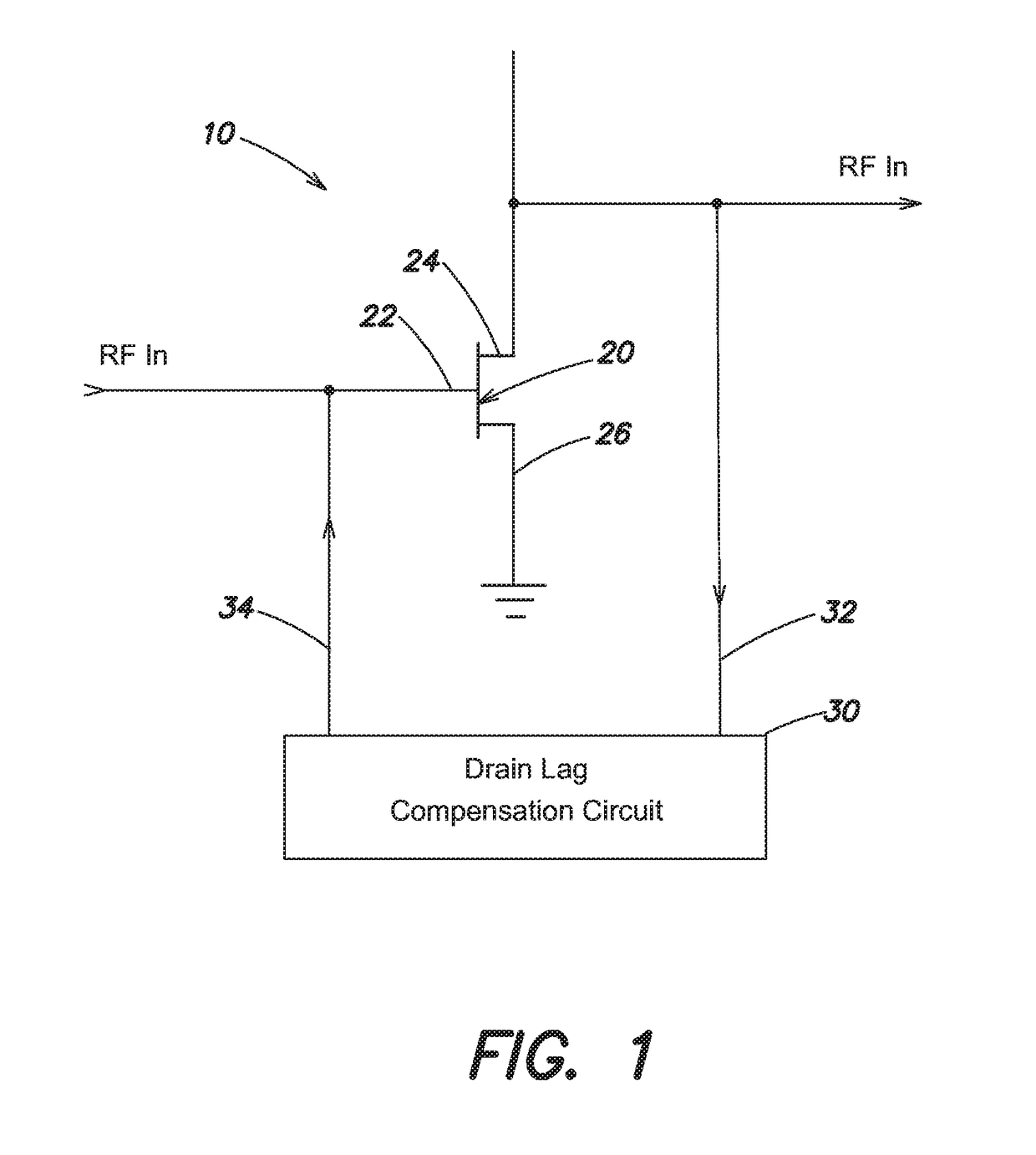
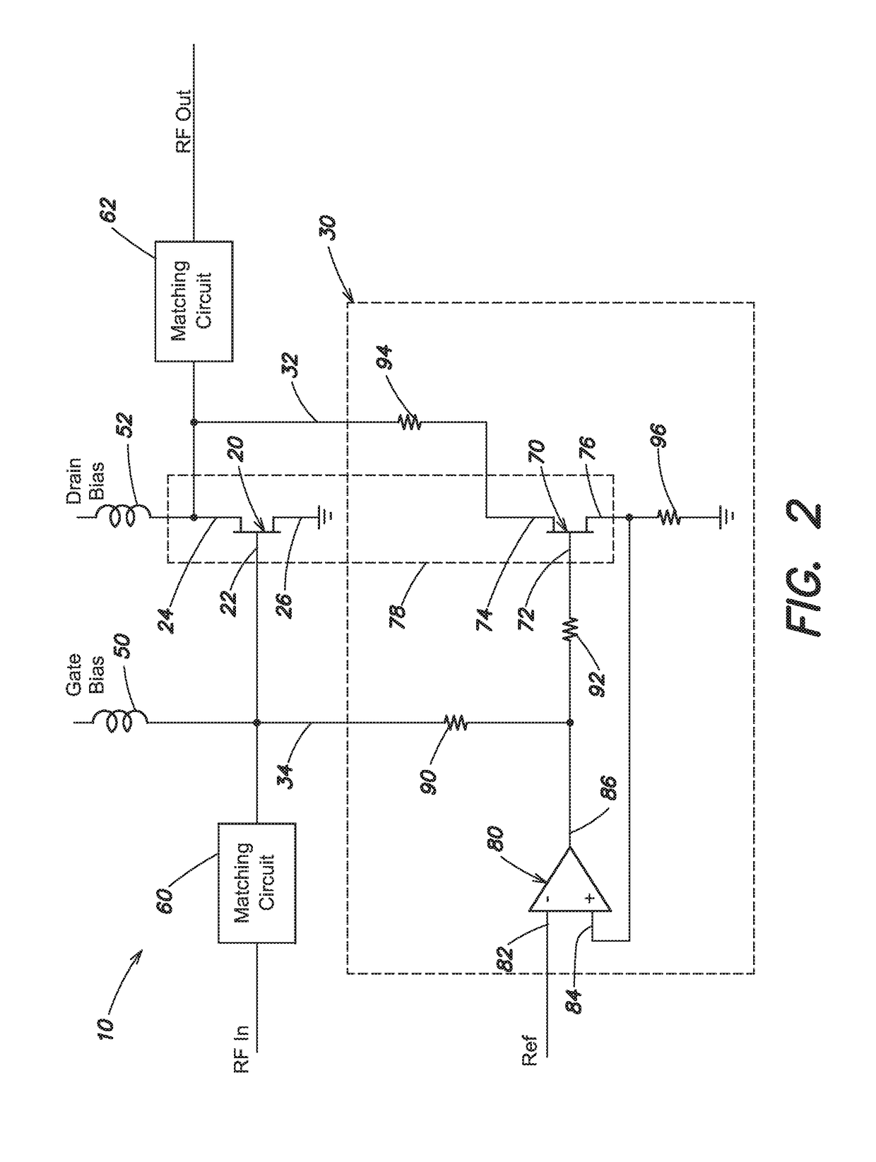
[0026]A schematic block diagram of a transistor circuit in accordance with embodiments is shown in FIG. 1. A transistor circuit 10 includes a transistor 20 and a drain lag compensation circuit 30. The transistor 20, referred to herein as a main transistor, is a component of an operating circuit, such as for example a power amplifier. Other components of the operating circuit are omitted for simplicity of illustration. Bias circuits and matching circuits are also omitted for simplicity of illustration. In some embodiments, the transistor 20 may be a gallium nitride (GaN) high electron mobility transistor (HEMT). However, transistor circuit 10 is not limited to gallium nitride HEMTs.

[0027]As shown, the transistor 20 includes a gate terminal 22, a drain terminal 24 and a source terminal 26. The source terminal 26 is connected to ground in the embodiment of FIG. 1. During operation, the transistor 20 receives an RF input signal on the gate terminal 22 and provides an RF output signal on...


PUM


Abstract

A transistor circuit includes a main transistor having a gate terminal, a drain terminal and a source terminal, and a drain lag compensation circuit configured to sense a drain voltage on the drain terminal of the main transistor and to control a drain current through the main transistor based on the sensed drain voltage. The drain lag compensation circuit may include a reference transistor having a drain terminal coupled to a drain terminal of the main transistor, and a sensing circuit that is coupled to a source terminal of the reference transistor and provides a control voltage to a gate terminal of the main transistor. The reference transistor may be thermally coupled to the main transistor. The main transistor may be a GaN RF power transistor.

Description

BACKGROUNDTechnical Field[0001]The disclosed technology relates to transistor circuits and, more particularly, to drain lag compensation circuits for RF (radio frequency) power transistors.Discussion of Related Art[0002]Gallium nitride transistors are used for radio frequency power amplifiers because they can operate at high temperatures and high voltage. Such devices may be used, for example, in the base station of a mobile phone system to output modulated signals.[0003]A mechanism that limits the performance of gallium nitride transistors is the trapping effect which causes a reduction in drain current after the application of a high voltage. This mechanism is described by Joh et al. in “A Current-Transient Methodology For Trap Analysis For GaN High Electron Mobility Transistors”, IEEE Transactions on Electron Devices, Vol. 58, No. 1, January 2011, pages 132-140. The trapping effect, also known as the drain lag effect, may change the characteristics of the transistor when a high a...

Claims


Application Information

Patent Timeline
Patent Type & Authority Applications(United States)
IPC IPC(8): H03K17/16H03F1/56H03F3/45H03F3/21H03F3/193
CPCH03K17/161H03F1/56H03F3/45H03F2200/387H03F3/193H03F2200/451H03F2200/222H03F3/21H03F1/30H03F1/34H03K17/063
Inventor LECKEY, JONATHAN
Owner MACOM TECH SOLUTIONS HLDG INC
Learn More