
Flat panel display

Active Publication Date: 2018-04-12
SAMSUNG DISPLAY CO LTD
View PDF0 Cites 8 Cited by
  • Summary
  • Abstract
  • Description
  • Claims
  • Application Information

AI Technical Summary

Benefits of technology

The patent text describes a flat panel display that can prevent an electrical short circuit when an integrated circuit chip is mounted on a substrate. Additionally, it provides a flat panel display where the mounting of an IC chip on the substrate is easy, and a complete electrical connection between the chip and the bonding pad can be formed.

Problems solved by technology

In this process, an unwanted electrical short circuit can occur between the IC chip and the bonding pad part or a power line, which can cause a failure.

Method used


Image

  • Flat panel display
  • Flat panel display
  • Flat panel display

Examples


Embodiment Construction

[0033]Exemplary embodiments will now be described more fully hereinafter with reference to the accompanying drawings; however, they may be embodied in different forms and should not be construed as limited to the embodiments set forth herein.

[0034]In the drawing figures, dimensions may be exaggerated for clarity of illustration. It will be understood that when an element is referred to as being “between” two elements, it can be the only element between the two elements, or one or more intervening elements may also be present. Like reference numerals may refer to like elements throughout.

[0035]Hereinafter, exemplary embodiments of the present disclosure will be described with reference to the accompanying drawings. However, it is to be understood by those skilled in the art that various modifications can be made in the following embodiments of the present invention, and the scope of the present invention is not limited to the following embodiments.

[0036]FIG. 1 is a schematic plan vie...


PUM


Abstract

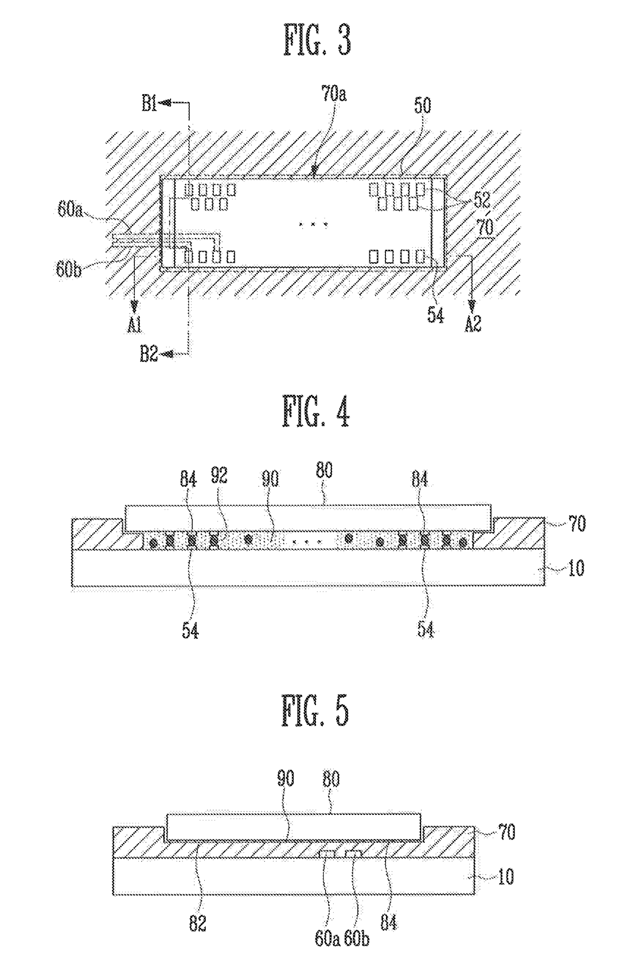
A flat panel display includes: a substrate that includes a display region and a non-display region at a periphery of the display region; a pixel array disposed on the substrate of the display region; an input pad part disposed on the substrate of the non-display region; a bonding pad part disposed on the substrate of the non-display region, the bonding pad part including a plurality of output pads connected to the pixel array and a plurality of input pads connected to the input pad part; and a protective layer disposed on the substrate of the non-display region, the protective layer having openings formed therein that expose portions of the bonding pad part and the input pad part, wherein the opening of the protective layer is smaller than the bonding pad part, wherein the protective layer is thinner at a portion that overlaps the bonding pad part than at other portions.

Description

CROSS REFERENCE TO RELATED APPLICATIONS[0001]The present application claims priority under 35 U.S.C. § 119 from, and the benefit of, Korean Patent Application No. 10-2016-0129106, filed on Oct. 6, 2016 in the Korean Intellectual Property Office, the contents of which are herein incorporated by reference in their entirety.BACKGROUND1. Technical Field[0002]Embodiments of the present disclosure are directed to a flat panel display, and more particularly, to a flat panel display in which a driving circuit is mounted in the form of an integrated circuit (IC) chip.2. Discussion of the Related Art[0003]In general, a flat panel display such as a liquid crystal display (LCD) or an organic light emitting display (OLED) is a display device that includes a pixel array. The pixel array includes a plurality of pixels. The plurality of pixels may be connected, for example, in a matrix form between scan and data lines.[0004]The pixel array is disposed in a display region of a substrate. A scan driv...

Claims


Application Information

Patent Timeline
IPC IPC(8): G09G3/20H01L27/32H01L51/52G09G3/22
CPCG09G3/2092H01L27/3276H01L51/5253H01L51/5203G09G3/22G09G3/2085G09G2300/0408G09G2300/0426G09G2300/0434G09G2300/0439G09F9/33G09F9/35G09G3/3208G09G3/36H10K59/873H10K59/131G09G3/006G09G3/3225G02F1/13458G02F1/13452H05K3/323H01L2924/12044H10K71/70H10K50/805H10K50/844
Inventor SO, DONG YOONPARK, KYUNG MIN
Owner SAMSUNG DISPLAY CO LTD
Learn More