Printed circuit board, electronic device, and manufacturing method of printed circuit board

Active Publication Date: 2018-03-29
CANON KK
View PDF1 Cites 4 Cited by
  • Summary
  • Abstract
  • Description
  • Claims
  • Application Information

AI Technical Summary

Benefits of technology

The present invention is a printed circuit board that improves its reliability, a method to manufacture it, and an electronic device that uses it. The invention results in smaller sizes and better performance of the electronic component.

Problems solved by technology

In this case, there may be an issue of ensuring the strength of the solder junction.
Further, since improvement of performance of an electronic component involves an increased heat value during operation resulting in larger deformation due to a thermal expansion, the thermal deformation may cause a disconnection to occur in the solder junction.
As discussed above, reduction in size and improvement of performance of an electronic component causes an issue of ensuring a junction reliability of a solder junction between a package and a printed wiring board.
In the arrangement in which the reinforcement lands are provided at four corners outside the area of the connection lands, however, the size of the package may increase.
Further, in the arrangement in which the reinforcement lands are provided at four corners inside the area of the connection lands, because of decrease in the number of signal terminals, a desired performance may not be obtained.
H8-139233, it may be difficult to achieve both reduction in size and improvement of performance of an electronic component.

Method used


Image

  • Printed circuit board, electronic device, and manufacturing method of printed circuit board
  • Printed circuit board, electronic device, and manufacturing method of printed circuit board
  • Printed circuit board, electronic device, and manufacturing method of printed circuit board

Examples


first embodiment

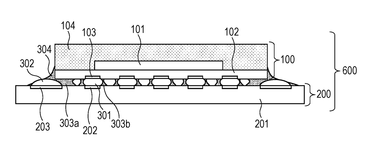
[0023]FIG. 1 is a sectional view of a printed circuit board 600 according to the first embodiment of the present invention. The printed circuit board 600 has a semiconductor device 100 and a printed wiring board 200 on which the semiconductor device 100 is mounted.

[0024]The semiconductor device 100 has a semiconductor element 101, a package substrate 102, and a mold resin 104. A plurality of lands 103 (first land) are provided on the bottom face of the semiconductor device 100, that is, the surface of the package substrate 102. The semiconductor device 100 is an electronic component having terminals of an LGA. The package substrate 102 is a substrate having an insulator formed of aluminum ceramics or the like and a conductive layer and has a function of electrically connecting the terminals of the semiconductor element 101 to the corresponding lands 103. The mold resin 104 is a resin formed so as to cover the semiconductor element 101 by using a fabrication method such as injection ...

second embodiment

[0054]FIG. 4 is a sectional view of a printed circuit board 620 according to the second embodiment of the present invention. FIG. 4 is different from FIG. 1 of the first embodiment in that the entire solder aggregation member 206 is provided outside the mounting region 105 of the semiconductor device 100, that is, outside the side face of the semiconductor device 100. Thus, solder 307 formed on the solder aggregation member 206 is also entirely located outside the mounting region 105 of the semiconductor device 100.

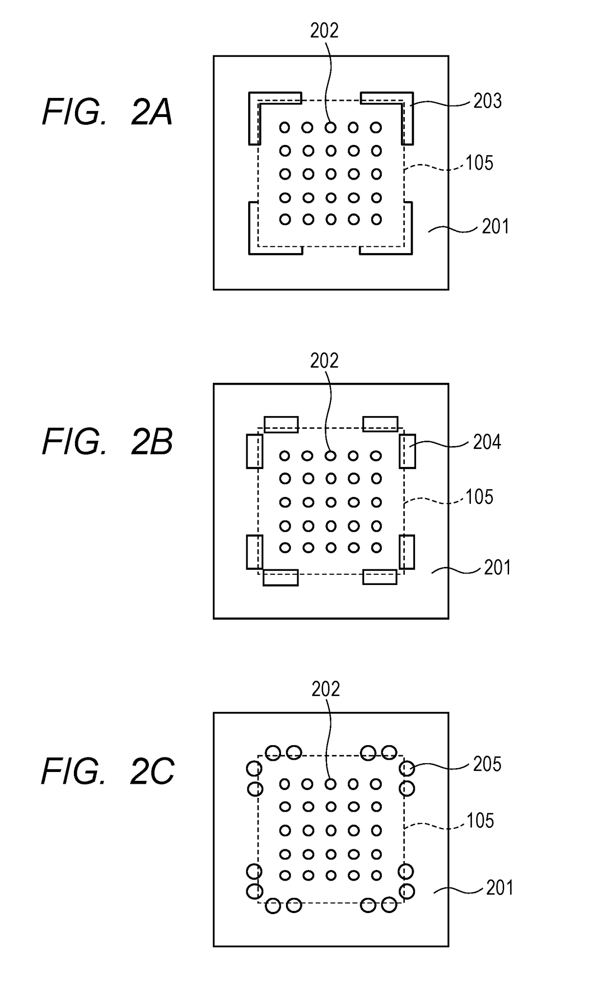
[0055]FIG. 5A, FIG. 5B, and FIG. 5C are examples of plan views of the printed wiring board 220. FIG. 5A, FIG. 5B, and FIG. 5C are drawings corresponding to FIG. 2A, FIG. 2B, and FIG. 2C of the first embodiment. While the solder aggregation member 203 is provided in a position extending over the inside and the outside of the mounting region 105 in FIG. 2A of the first embodiment, the entire solder aggregation member 206 is provided outside the mounting region 105 in FIG. 5...

third embodiment

[0058]FIG. 7A to FIG. 7D are sectional views illustrating the manufacturing process of the printed circuit board 640 according to the third embodiment. FIG. 7A to FIG. 7D are different from FIG. 6A to FIG. 6D of the second embodiment in that a semiconductor device 120 is an electronic component having terminals of a BGA. The semiconductor device 120 has solder balls 106 each formed on corresponding one of the plurality of lands 103. Since other features are the same as those in the second embodiment, the description thereof will be omitted.

[0059]According to the present embodiment, the same advantages as those in the first embodiment and the second embodiment can be obtained also in the electronic component having terminals of a BGA.

[0060]Note that, when supplying the thermosetting resin-containing solder paste 401a, it is desirable that the height of the supplied thermosetting resin-containing solder paste 401a be higher than the solder balls 106. The reasons thereof are as follows...


PUM


Abstract

Provided is a printed circuit board including: an electronic component having a bottom face and a side face, in which first lands are provided on the bottom face; a printed wiring board having a mounting face, in which second lands corresponding to the first lands are provided on the mounting face, and in which the electronic component is mounted such that the bottom face faces the mounting face; a solder aggregation member provided outside the second lands on the mounting face; pieces of first solder each of which joins each of the first lands to corresponding one of the second lands; second solder formed on the solder aggregation member; and a thermosetting resin adhered to the bottom face of the electronic component outside the first lands and to the mounting face of the printed wiring board outside the second lands.

Description

BACKGROUND OF THE INVENTIONField of the Invention[0001]The present invention relates to a printed circuit board, an electronic device, and a manufacturing method of the printed circuit board.Description of the Related Art[0002]In recent years, reduction in size and improvement of performance of electronic devices have involved a reduction in size and an improvement of performance of electronic components mounted on a printed wiring board used in the electronic devices.[0003]Packages such as a ball grid array (BGA), a land grid array (LGA), and the like that allows for a reduction in size and an increase in the number of terminals are widely used in electronic components used in an electronic device such as a mobile device, a digital camera, or the like.[0004]Since the BGA and the LGA have the structure in which electrodes are provided on the bottom face of the package, no lead terminal is needed allowing for a reduction in size. Further, with a smaller pitch of the electrodes on the...

Claims


Application Information

Patent Timeline
IPC IPC(8): H05K1/18H05K1/11H05K3/30H05K3/34
CPCH05K1/181H05K1/111H05K2201/2081H05K3/341H05K3/3484H05K3/305H05K3/3489H05K2203/0485H05K3/3436H05K3/3463H05K2201/09409B23K35/262B23K35/3613B23K35/0222B23K35/0244H05K3/3485Y02P70/50
Inventor MINEGISHI, KUNIHIKO
Owner CANON KK
Why Eureka
Try Eureka