
Resistor element and resistor element assembly

a resistor element and element technology, applied in the direction of resistor details, resistor chip manufacture, circuit electrostatic discharge protection, etc., can solve the problems of resistor element damage, signal distortion and circuit damage, and the like, and achieve the effect of improving anti-surge performan

Active Publication Date: 2018-03-01
SAMSUNG ELECTRO MECHANICS CO LTD
View PDF0 Cites 4 Cited by
  • Summary
  • Abstract
  • Description
  • Claims
  • Application Information

AI Technical Summary

Benefits of technology

The patent is about a resistor element that can make it harder for electronic components to be damaged by sudden surges of electricity. This element can be used in a resistor element assembly.

Problems solved by technology

Electronic apparatuses that have been digitized and operate at increased speeds are sensitive to external stimuli, such that signal distortion and circuit damage may occur due to external noise.
Particularly, portable electronic apparatuses such as smartphones, tablet personal computers (PC), and the like, are frequently exposed to external impacts such as electrostatic discharge (ESD) or electromagnetic waves.
Abnormal voltage, such as ESD, in a circuit containing the resistor element can cause damage within the resistor element, such as a short circuit.
In such a case, all of the current of a power supply flows to an integrated circuit (IC), which causes secondary damage to the IC.
However, that design inevitably increases the space occupied by the plurality of resistors.

Method used


Image

  • Resistor element and resistor element assembly
  • Resistor element and resistor element assembly
  • Resistor element and resistor element assembly

Examples


Embodiment Construction

[0022]Hereinafter, exemplary embodiments of the present disclosure will now be described in detail with reference to the accompanying drawings.

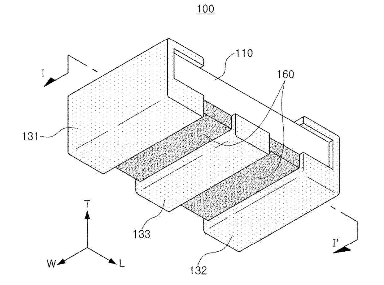
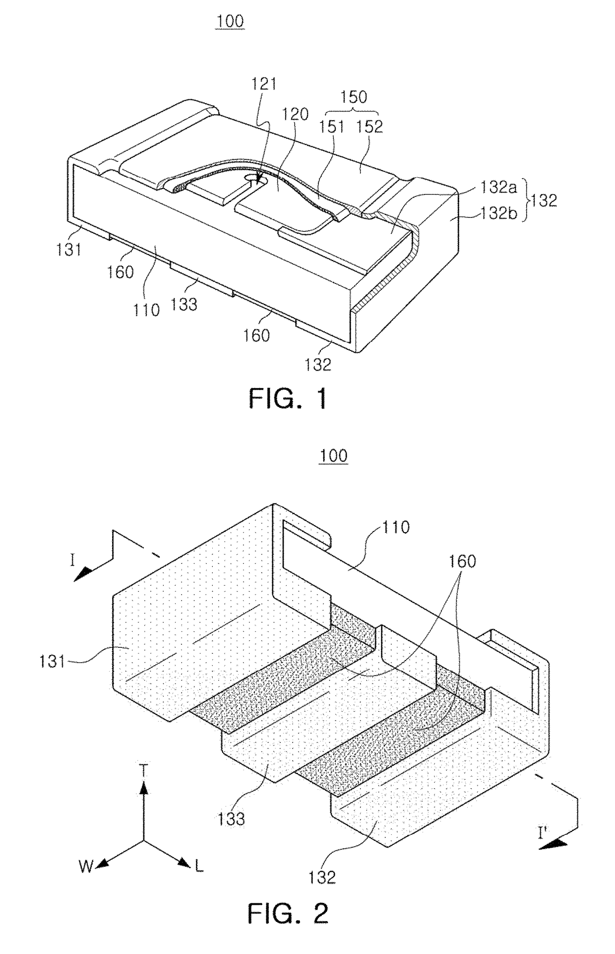
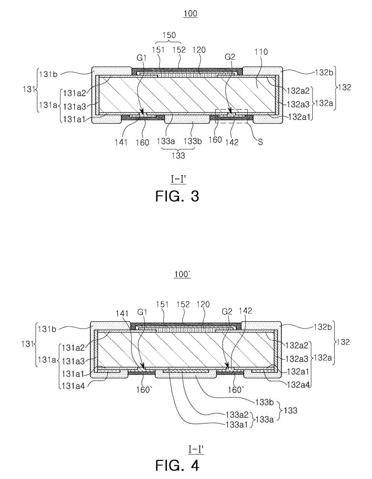
[0023]FIG. 1 is a perspective and partial cross-section view illustrating an exemplary embodiment of a resistor element. FIG. 2 is a perspective view illustrating the resistor element of FIG. 1 when viewed from another viewpoint. FIG. 3 is a cross-sectional view illustrating the exemplary embodiment of FIG. 1 taken along line I-I′ of FIG. 2.

[0024]Referring to FIGS. 1 through 3, a resistor element 100 includes a base substrate 110, a resistor layer 120, first to third terminals 131 to 133, and electrostatic discharge (ESD)-preventing members 141 and 142.

[0025]The base substrate 110 supports the resistor layer 120 and secures the strength of the resistor element 100. The base substrate 110 has a predetermined thickness and has a thin plate shape that includes first and second surfaces opposing each other and each having a rectangular shape, but...


PUM


Abstract

A resistor element includes a base substrate having first and second surfaces opposing each other; a resistor layer disposed on the first surface of the base substrate; first and second terminals disposed on opposing end portions of the base substrate, respectively, and electrically connected to opposing sides of the resistor layer, respectively; a third terminal disposed between the first terminal and the second terminal on the second surface of the base substrate and spaced apart from the first terminal and the second terminal; and electrostatic discharge (ESD)-preventing members connecting the first terminal and the third terminal to each other and connecting the second terminal and the third terminal to each other.

Description

CROSS-REFERENCE TO RELATED APPLICATION(S)[0001]This application claims the benefit of priority to Korean Patent Application Nos. 10-2016-0110456 filed on Aug. 30, 2016 and 10-2016-0118386 filed on Sep. 13, 2016 in the Korean Intellectual Property Office, the entire disclosures of which are incorporated herein by reference for all purposes.BACKGROUND1. Field[0002]The present disclosure relates to a resistor element and a resistor element assembly.2. Description of Related Art[0003]Electronic apparatuses that have been digitized and operate at increased speeds are sensitive to external stimuli, such that signal distortion and circuit damage may occur due to external noise.[0004]Particularly, portable electronic apparatuses such as smartphones, tablet personal computers (PC), and the like, are frequently exposed to external impacts such as electrostatic discharge (ESD) or electromagnetic waves.[0005]A resistor element with a chip shape is appropriate for implementing a precise degree o...

Claims


Application Information

Patent Timeline
Patent Type & Authority Applications(United States)
IPC IPC(8): H01C1/06H01C1/14H01C1/012
CPCH01C1/06H01C1/012H01C1/14H01C1/142H01C1/148H01C7/003H01C17/006H05K1/0259H05K2201/10022
Inventor PARK, KWANG HYUNKIM, HAE IN
Owner SAMSUNG ELECTRO MECHANICS CO LTD
Learn More