Optical receiver, optical transceiver, and optical signal reception control method

a technology of optical transceiver and optical receiver, applied in the direction of electromagnetic transceivers, multi-component communication, wavelength-division multiplex systems, etc., can solve the problems of difficult disposal of soa and voa

Active Publication Date: 2018-01-04
FUJITSU OPTICAL COMPONENTS LTD
View PDF4 Cites 6 Cited by
  • Summary
  • Abstract
  • Description
  • Claims
  • Application Information

AI Technical Summary

Benefits of technology

[0008]According to an aspect of an embodiment, an optical receiver includes a demultiplexer configured to demultiplex, for each channel, optical signals input through a plurality of channels; a photoelectric converter having a number of light receivers corresponding to the plurality of channels, the photoelectric converter being configured to convert an optical signal into an electric signal for each channel; a monitor circuit configured to monitor, for each channel, an amplitude characteristic of the optical signal converted into the electric signal by the photoelectric converter; and a control circuit configured to control, based on a monitored result of the monitor circuit, a bias voltage to be applied to the light receiver such that an amount of variability in the amplitude characteristic between the channels is minimum or falls within a predetermined range.

Problems solved by technology

However, for an objective of downscaling CFP 4 and QSFP 28, the SOA and VOA may be difficult to be disposed due to constraints of mounting sizes.

Method used


Image

  • Optical receiver, optical transceiver, and optical signal reception control method
  • Optical receiver, optical transceiver, and optical signal reception control method
  • Optical receiver, optical transceiver, and optical signal reception control method

Examples


first embodiment

Modification of First Embodiment

[0061]The configuration and method of the first embodiment are not limited to the examples described above. As the reference channel among the multiple channels, a channel in which the maximum photocurrent flows may be selected instead of the channel with the minimum current value. When priority is given to reducing the amount of noise with respect to other channels, the S / N ratio is optimized by setting the channel with the smallest current monitor value to the reference channel and matching the voltage values of the other channels to the photocurrent multiplication factor of the reference channel. However, for accurate data detection it is desirable to have an input power that is greater than a certain level. Hence, control to optimize the S / N ratio by matching the photocurrent amounts of multiple channels to the maximum current monitor value is also effective for reducing the effect of crosstalk. In this case, for example, the ratio of the current ...

second embodiment

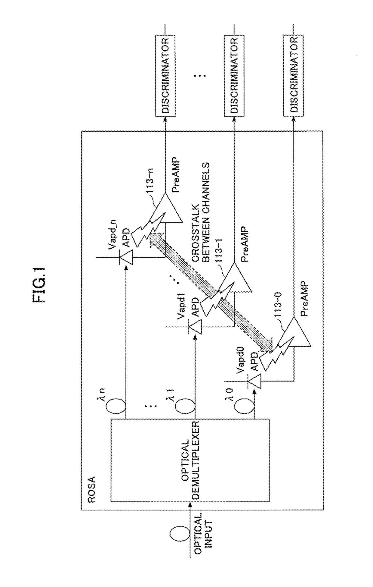
[0067]FIG. 10 is a schematic diagram of an optical receiver 10B of a second embodiment. In the second embodiment, the amplitudes of the voltage signals output from the preamplifiers 113-0 to 113-n are monitored instead of monitoring the photocurrent flowing in the APD, and voltage control is performed based on the monitored results.

[0068]The optical receiver 10B includes an optical reception module 11B, power supply circuits 15-0 to 15-n, and amplitude detection circuits 115-0 to 115-n as monitor circuits. In the optical receiver 10B, a clock data recovery (CDR) 12, a temperature detection circuit 17, and a control integrated circuit (IC) 30 are also used; however, these components may be used in common with an optical transmitter in an optical transceiver.

[0069]Similar to the first embodiment, in the optical reception module 11B, multichannel input optical signals are demultiplexed into respective channels by the optical demultiplexer 111 and the demultiplexed optical signals are p...

third embodiment

[0080]FIG. 13 depicts a flowchart of voltage control of a third embodiment.

[0081]Since a multiplication factor of the photocurrent of the APDs 112-0 to 112-n has temperature dependency, control corresponding to a temperature change may be incorporated in bias control that reduces the effect of crosstalk.

[0082]FIGS. 14A and 14B are graphs illustrating temperature dependency of a photocurrent multiplication factor of the APD. FIG. 14A is a diagram illustrating a relationship between APD bias voltage (Vapd) and photocurrent (Iapd) at different temperatures, and FIG. 14B a diagram illustrating a relationship between temperature (T) and bias voltage (VB). As illustrated in FIG. 14A, a slope of a photocurrent change with respect to the applied bias voltage is greater at a low temperature side. As described in the first embodiment, by using one reset change amount, which is adjusted in advance to the low temperature side, the optimum multiplication factor may also be achieved, while repeat...


PUM


Abstract

An optical receiver includes a demultiplexer configured to demultiplex, for each channel, optical signals input through a plurality of channels, a photoelectric converter having a number of light receivers corresponding to the plurality of channels, the photoelectric converter being configured to convert an optical signal into an electric signal for each channel, a monitor circuit configured to monitor, for each channel, an amplitude characteristic of the optical signal converted into the electric signal by the photoelectric converter, and a control circuit configured to control, based on a monitored result of the monitor circuit, a bias voltage to be applied to the light receiver such that an amount of variability in the amplitude characteristic between the channels is minimum or falls within a predetermined range.

Description

CROSS-REFERENCE TO RELATED APPLICATION[0001]This patent application is based upon, and claims the benefit of priority of Japanese Patent Application No. 2016-131939 filed on Jul. 1, 2016, the entire contents of which are incorporated herein by reference.FIELD[0002]The embodiments discussed herein relate to an optical receiver, an optical transceiver using the optical receiver, and an optical signal reception control method.BACKGROUND[0003]In high-speed optical communication such as 100 Gigabit Ethernet (registered trademark), standardized optical modules such as CFPx and QSFP 28 are adopted by client side terminals. In order to achieve desired transmission speeds, these optical modules adopt a transmission scheme using amplitude modulation (AM) with 25 Gbps×4 channels (4 wavelengths). In the receiver optical subassembly (ROSA) used for photoelectric conversion and amplification at the receiver's side, four channels are integrated in one package for downscaling.[0004]In the ER4 stand...

Claims


Application Information

Patent Timeline
Patent Type & Authority Applications(United States)
IPC IPC(8): H04J14/02H04B10/69H04B10/40
CPCH04J14/0221H04B10/40H04B10/69H04B10/671H04B10/6911
Inventor ISHII, TOSHIO
Owner FUJITSU OPTICAL COMPONENTS LTD
Why Eureka
Try Eureka