
Semiconductor device and display device including the semiconductor device

a semiconductor and display device technology, applied in the direction of semiconductor devices, electrical devices, transistors, etc., can solve the problems of affecting the characteristics of transistors, reducing the number of transistors, and reducing the image quality of the display device, so as to achieve stable semiconductor characteristics, low manufacturing cost, and relatively simple manufacturing process

Active Publication Date: 2017-12-28
SEMICON ENERGY LAB CO LTD
View PDF2 Cites 2 Cited by
  • Summary
  • Abstract
  • Description
  • Claims
  • Application Information

AI Technical Summary

Benefits of technology

This patent is about improving the reliability and performance of transistors made with oxide semiconductor films. The invention provides a staggered transistor structure that suppresses changes in electrical characteristics and has high reliability, high on-state current, low off-state current, and low power consumption. Furthermore, the invention provides a novel semiconductor device that overcomes limitations of existing devices.

Problems solved by technology

However, an inverted staggered transistor has the following drawback: as the screen size of a display device increases or the resolution of an image of a display device increases, a typical example of which is a high-resolution display device with 4K×2K pixels (3840 pixels in the horizontal direction and 2160 pixels in the vertical direction) or 8K×4K pixels (7680 pixels in the horizontal direction and 4320 pixels in the vertical direction), signal delay or the like due to parasitic capacitance between a gate electrode and source and drain electrodes of the transistor becomes more severe, and accordingly, the image quality of the display device degrades.
Furthermore, in the case where a transistor is formed using an oxide semiconductor film for a channel region, an oxygen vacancy which is formed in the channel region of the oxide semiconductor film adversely affects the transistor characteristics.
Furthermore, there is a problem in that electrical characteristics vary among transistors.

Method used


Image

  • Semiconductor device and display device including the semiconductor device
  • Semiconductor device and display device including the semiconductor device
  • Semiconductor device and display device including the semiconductor device

Examples


embodiment 1

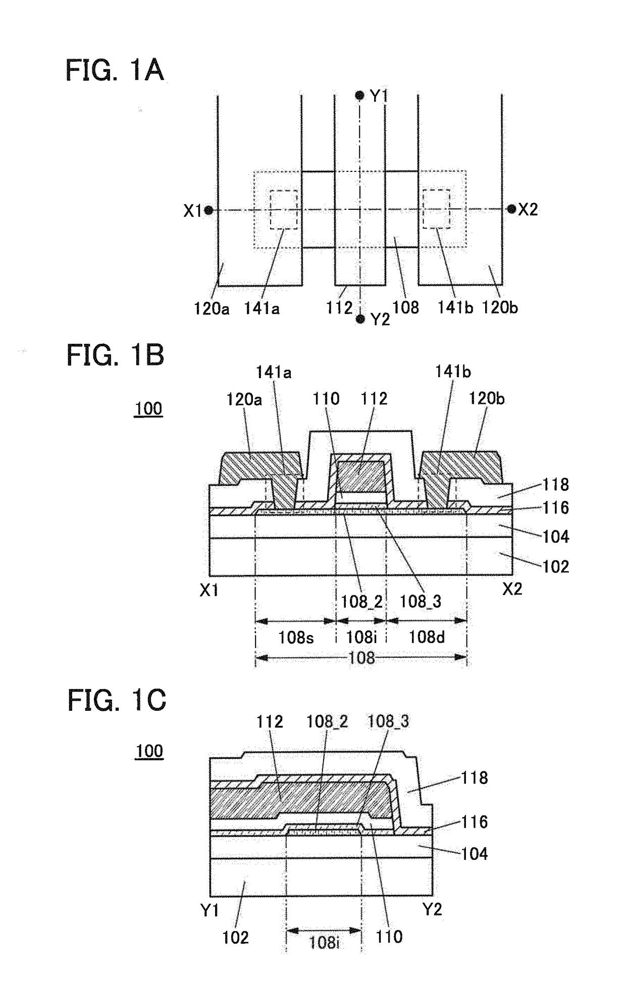
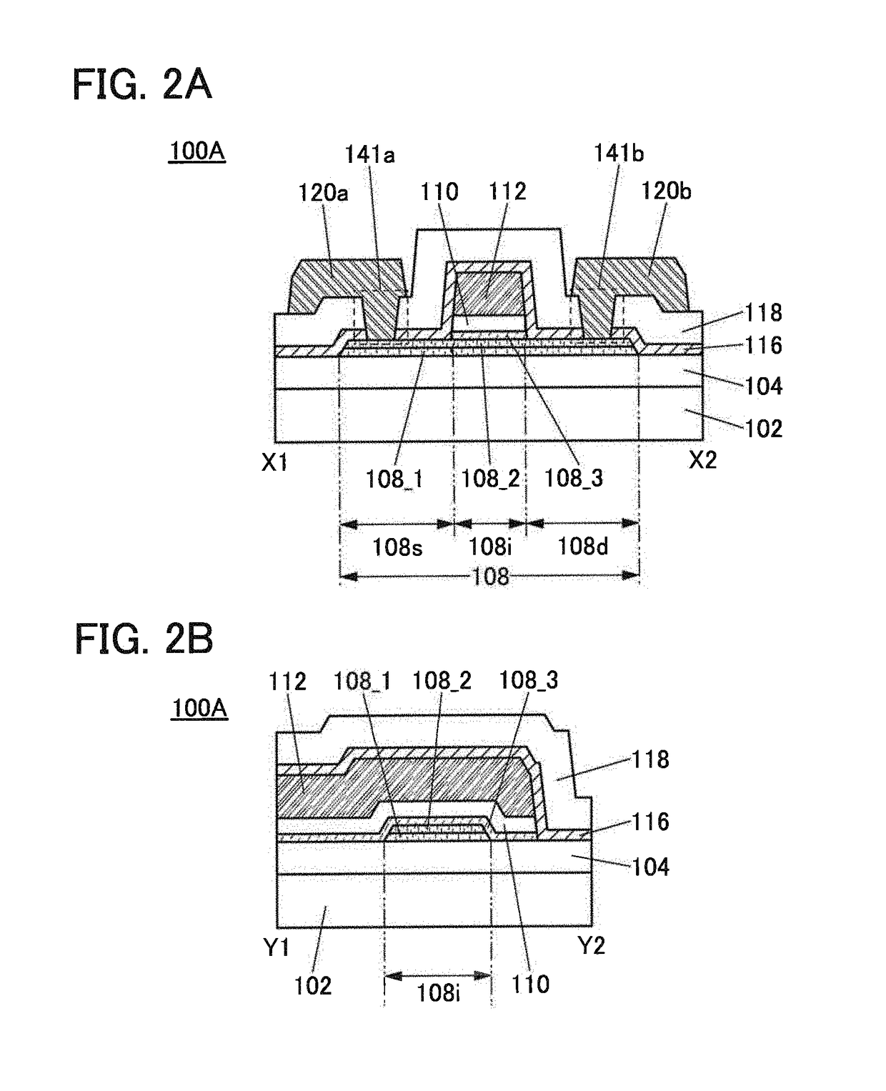
[0080]In this embodiment, examples of a semiconductor device including a transistor and a method for manufacturing the semiconductor device will be described with reference to FIGS. 1A to 22C.

1-1. Structural Example 1 of Semiconductor Device

[0081]FIGS. 1A to 1C illustrate an example of a semiconductor device including a transistor. Note that the transistor in FIGS. 1A to 1C has a top-gate structure.

[0082]FIG. 1A is a top view of a transistor 100. FIG. 1B is a cross-sectional view taken along dashed-dotted line X1-X2 in FIG. 1A. FIG. 1C is a cross-sectional view taken along dashed-dotted line Y1-Y2 in FIG. 1A. For clarity, FIG. 1A does not illustrate some components such as an insulating film 110. As in FIG. 1A, some components are not illustrated in some cases in top views of transistors described below. Furthermore, the direction of dashed-dotted line X1-X2 may be referred to as a channel length (L) direction, and the direction of dashed-dotted line Y1-Y2 may be referred to as a ch...

embodiment 2

[0318]In this embodiment, the structure and the like of an oxide semiconductor will be described with reference to FIGS. 23A to 23E, FIGS. 24A to 24E, FIGS. 25A to 25D, FIGS. 26A and 26B, and FIG. 27.

2-1. Structure of Oxide Semiconductor

[0319]An oxide semiconductor is classified into a single-crystal oxide semiconductor and a non-single-crystal oxide semiconductor. Examples of the non-single-crystal oxide semiconductor include a c-axis aligned crystalline oxide semiconductor (CAAC-OS), a polycrystalline oxide semiconductor, a nanocrystalline oxide semiconductor (nc-OS), an amorphous-like oxide semiconductor (a-like OS), and an amorphous oxide semiconductor.

[0320]From another perspective, an oxide semiconductor is classified into an amorphous oxide semiconductor and a crystalline oxide semiconductor. Examples of the crystalline oxide semiconductor include a single-crystal oxide semiconductor, a CAAC-OS, a polycrystalline oxide semiconductor, and an nc-OS.

[0321]An amorphous structure ...

embodiment 3

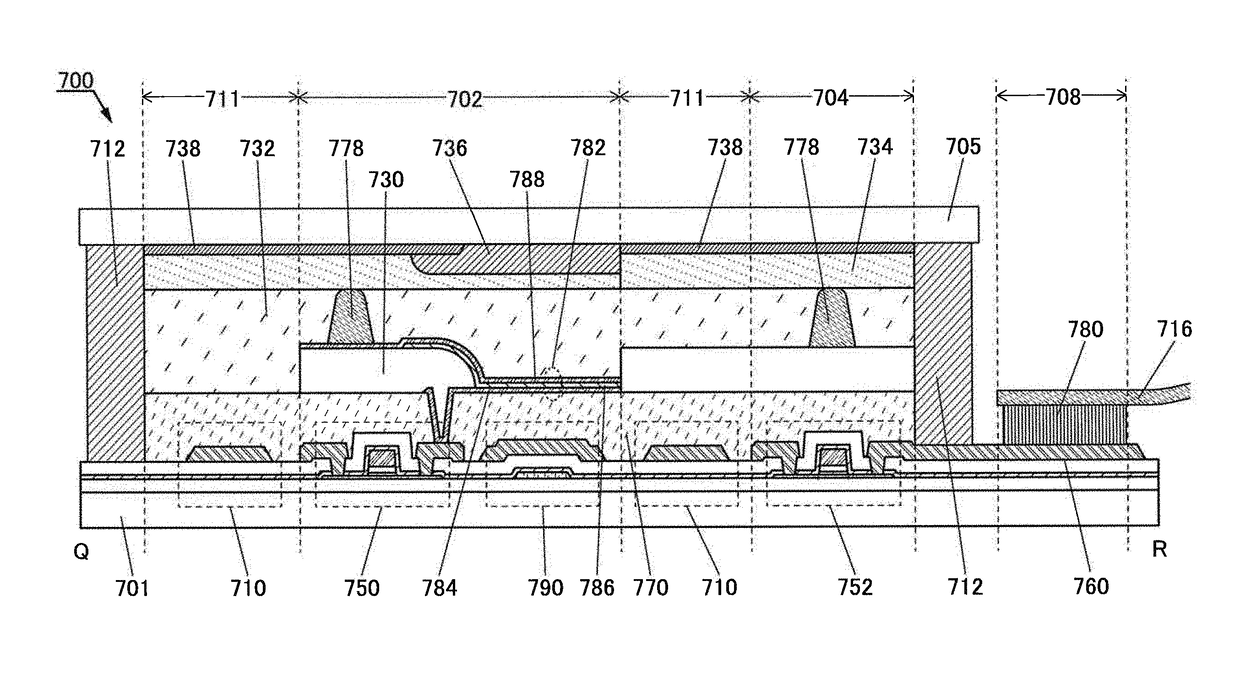
[0360]In this embodiment, an example of a display device that includes the transistor described in the above embodiment will be described below with reference to FIG. 28, FIG. 29, and FIG. 30.

[0361]FIG. 28 is a top view illustrating an example of a display device. A display device 700 in FIG. 28 includes a pixel portion 702 provided over a first substrate 701, a source driver circuit portion 704 and a gate driver circuit portion 706 which are provided over the first substrate 701, a sealant 712 provided to surround the pixel portion 702, the source driver circuit portion 704, and the gate driver circuit portion 706, and a second substrate 705 provided to face the first substrate 701. The first substrate 701 and the second substrate 705 are sealed with the sealant 712. That is, the pixel portion 702, the source driver circuit portion 704, and the gate driver circuit portion 706 are enclosed by the first substrate 701, the sealant 712, and the second substrate 705. Although not illust...


PUM


Abstract

The reliability of a transistor including an oxide semiconductor is improved. The transistor in a semiconductor device includes a first oxide semiconductor film over a first insulating film, a gate insulating film over the first oxide semiconductor film, a second oxide semiconductor film over the gate insulating film, and a second insulating film over the first oxide semiconductor film and the second oxide semiconductor film. The first oxide semiconductor film includes a channel region overlapping with the second oxide semiconductor film, a source region and a drain region each in contact with the second insulating film. The channel region includes a first layer and a second layer in contact with a top surface of the first layer and covering a side surface of the first layer in the channel width direction. The second oxide semiconductor film has a higher carrier density than the first oxide semiconductor film.

Description

CROSS-REFERENCE TO RELATED APPLICATIONS[0001]This application is a continuation of U.S. application Ser. No. 15 / 160,059, filed May 20, 2016, now allowed, which claims the benefit of a foreign priority application filed in Japan as Serial No. 2015-104495 on May 22, 2015, both of which are incorporated by reference.TECHNICAL FIELD[0002]One embodiment of the present invention relates to a semiconductor device including an oxide semiconductor film and a display device including the semiconductor device.[0003]Note that one embodiment of the present invention is not limited to the above technical field. The technical field of one embodiment of the invention disclosed in this specification and the like relates to an object, a method, or a manufacturing method. In addition, the present invention relates to a process, a machine, manufacture, or a composition of matter. In particular, one embodiment of the present invention relates to a semiconductor device, a display device, a light-emitting...

Claims


Application Information

Patent Timeline
Patent Type & Authority Applications(United States)
IPC IPC(8): H01L29/786H01L29/24H01L27/12H01L29/66H01L29/04
CPCH01L29/78648H01L29/66969H01L29/78693H01L29/66742H01L29/786H01L29/24H01L27/1225H01L29/045H01L29/78696H01L29/7869H01L29/42364H01L29/42372H01L29/42384
Inventor KOEZUKA, JUNICHIJINTYOU, MASAMISHIMA, YUKINORI
Owner SEMICON ENERGY LAB CO LTD
Learn More