Packaging structure for OLED device and display apparatus

a technology of packaging structure and oled device, which is applied in the direction of basic electric elements, electrical apparatus, semiconductor devices, etc., can solve the problems of easy defect formation, difficult to isolate the packaging structure of oled device from water, oxygen and other ingredients in the air, and difficult to spread the organic layer formed of organic material

Active Publication Date: 2017-09-07
BOE TECH GRP CO LTD +1
View PDF5 Cites 6 Cited by
  • Summary
  • Abstract
  • Description
  • Claims
  • Application Information

AI Technical Summary

Benefits of technology

The patent describes a packaging structure for OLED devices that includes multiple layers of alternating inorganic and organic layers. The inorganic layers in contact with the OLED device have a smaller contact angle with the organic layer, allowing the organic layer to spread effectively on the inorganic layer. This prevents defects in the inorganic layer and ensures the OLED device is isolated from water, oxygen, and other air ingredients, increasing its service life. The packaging structure is also easy to apply and has good applicability for display apparatuses.

Problems solved by technology

However, due to the large difference in wettability between the SiNx material and the organic material, resulting in large contact angle between the SiNx material and the organic material, it is difficult for the organic layer formed of the organic material to sufficiently spread on the inorganic layer formed of the SiNx material.
Therefore, it is easy to form defects such as small holes in the organic layer, and the packaging structure cannot isolate the OLED device from water, oxygen and other ingredients in the air.
As a result, the service life of the OLED device will be decreased.
However, such methods are expensive and would lengthen the unit production time of the production line.
Accordingly, the applicability of above methods is poor.

Method used


Image

  • Packaging structure for OLED device and display apparatus
  • Packaging structure for OLED device and display apparatus
  • Packaging structure for OLED device and display apparatus

Examples


Embodiment Construction

[0022]In order to make the technical solutions and advantages of the embodiments of the disclosure clearer, a clear and complete description to the technical solutions of the embodiments of the disclosure will be made hereinafter in conjunction with drawings of the embodiments of the disclosure. Obviously, the embodiments described are only some of rather than all of the embodiments of the disclosure. All other embodiments obtained by one of ordinary skill in the art based on the embodiments described herein without any creative work will all fall into the scope claimed by the disclosure.

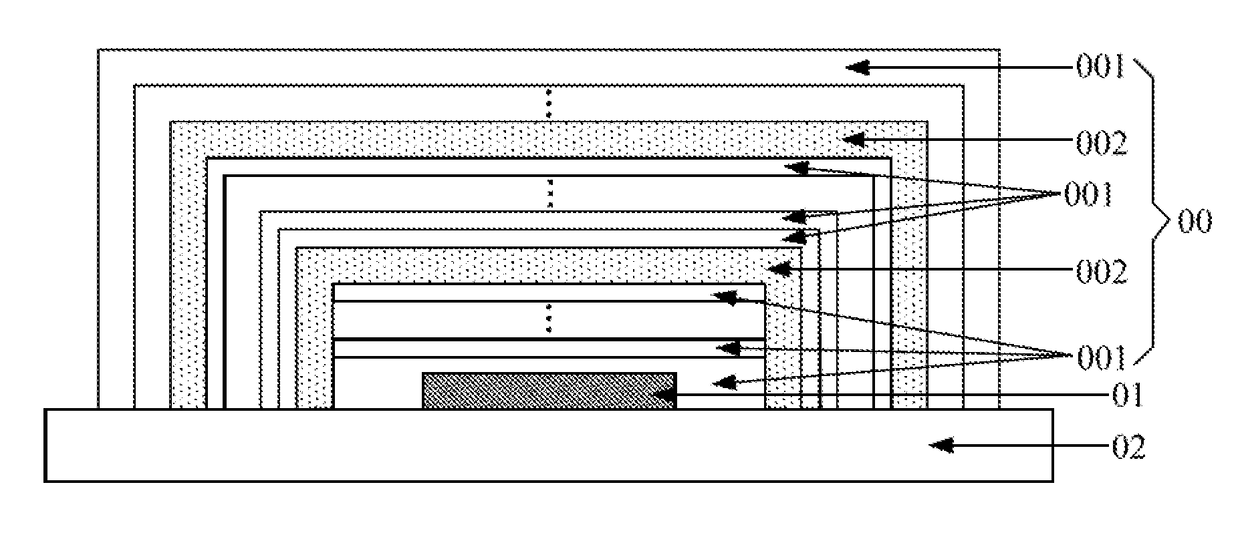
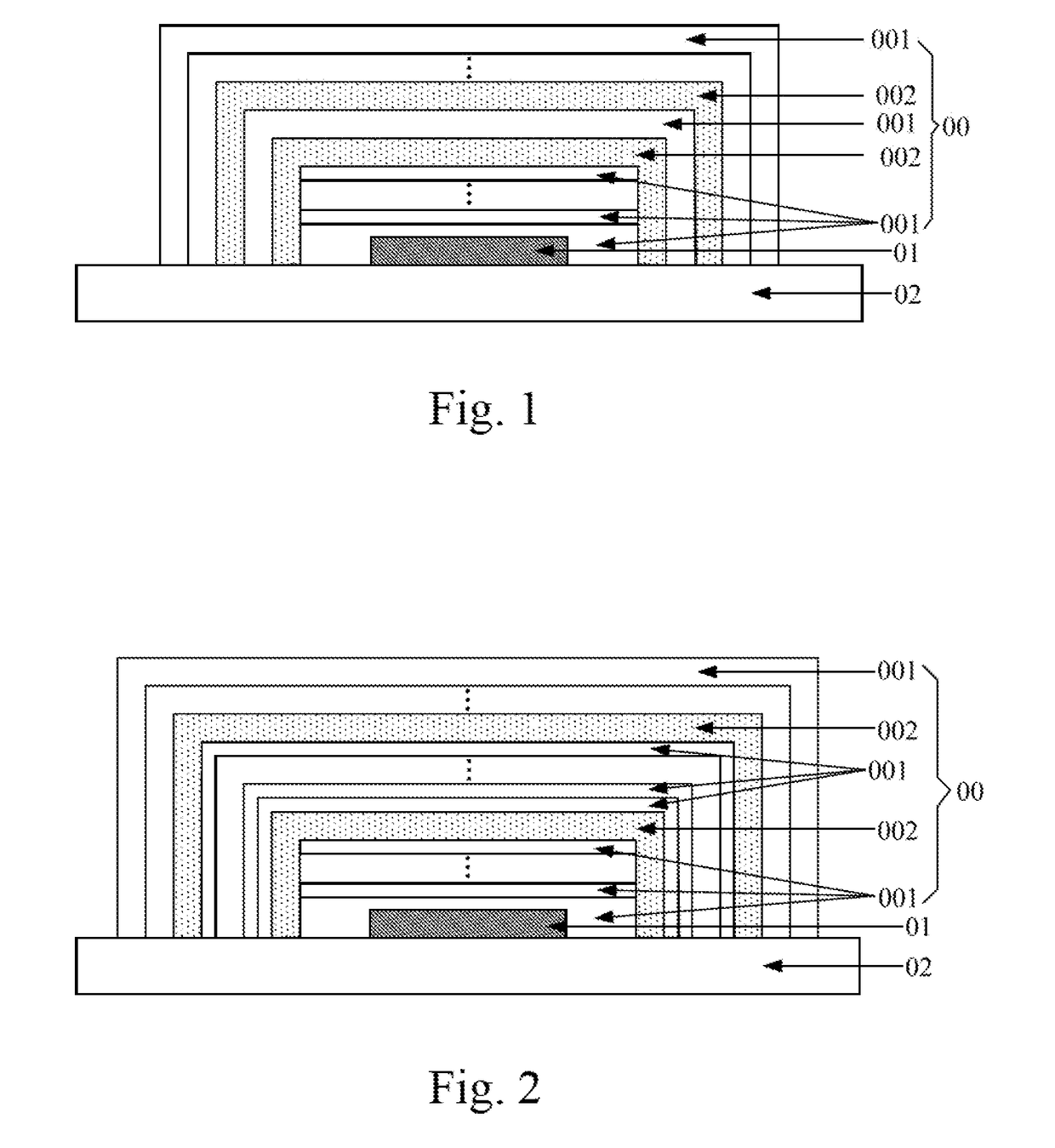
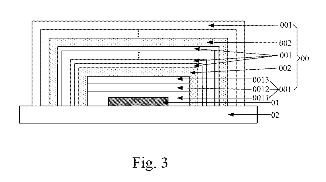
[0023]FIG. 1 is a schematic diagram illustrating a packaging structure 00 for OLED device provided on outer side of an OLED device 01 according to an embodiment. With reference to FIG. 1, the packaging structure 00 for OLED device includes a plurality of films coated on outer side of the OLED device 01 which includes alternately stacked inorganic layers 001 and organic layers 002. Among the pluralit...


PUM


Abstract

A packaging structure for an OLED device is provided. The packaging structure includes a plurality of films coated on an outer side of the OLED device and comprising alternately stacked inorganic layers and organic layers, wherein both a film in contact with the OLED device and a film farthest from the OLED device are inorganic layers, wherein the inorganic layer in contact with the OLED device comprises at least two sub-films sequentially stacked, and wherein a contact angle between i) a material for forming a sub-film of the at least two sub-films that contacts an organic layer and ii) an organic material for forming the organic layer is smaller than a preset angle.

Description

CROSS REFERENCE TO RELATED APPLICATIONS[0001]This application claims the benefit and priority of Chinese Patent Application No. 201610119026.7 filed on Mar. 2, 2016. The entire disclosure of the above application is incorporated herein by reference.BACKGROUND[0002]Embodiments described herein relate to a packaging structure for OLED device and a display apparatus.[0003]Organic light-emitting diode (referred to as OLED) devices are widely used in the display industry since they have such advantages as solid-state structure, high brightness, full view angle, rapid response speed and capability of flexible display, etc. However, the water, oxygen and other ingredients in the air have a great influence on the life of the OLED device. Thus, in order to increase the service life of an OLED device, it is usually necessary to package the OLED device by using a packaging structure to isolate the OLED device from water, oxygen and other ingredients in the air.[0004]In the prior art, a packagi...

Claims


Application Information

Patent Timeline
Patent Type & Authority Applications(United States)
IPC IPC(8): H01L51/52H01L51/56
CPCH01L51/56H01L51/5256H10K71/00H10K59/8731H10K50/8445
Inventor XIAO, ANGSHIN, HYUN CHELSUN, QUANQINWANG, XIANGNANCUI, FUYI
Owner BOE TECH GRP CO LTD
Why Eureka
Try Eureka