Imaging device and electronic device
a technology of electronic devices and imaging devices, applied in the direction of radiation controlled devices, optical radiation measurement, instruments, etc., can solve the problem of low use efficiency of incident light, and achieve the effect of reducing power consumption and increasing the speed of imaging devices
- Summary
- Abstract
- Description
- Claims
- Application Information
AI Technical Summary
Benefits of technology
Problems solved by technology
Method used
Image
Examples
embodiment 1
[0082]In this embodiment, an imaging device that is one embodiment of the present invention is described with reference to drawings.
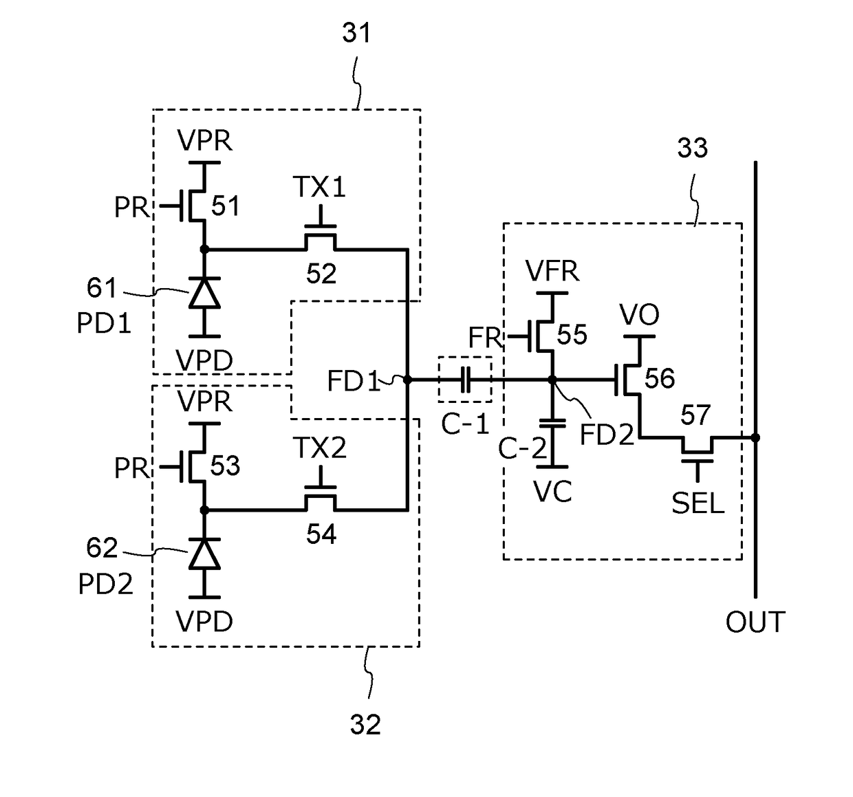
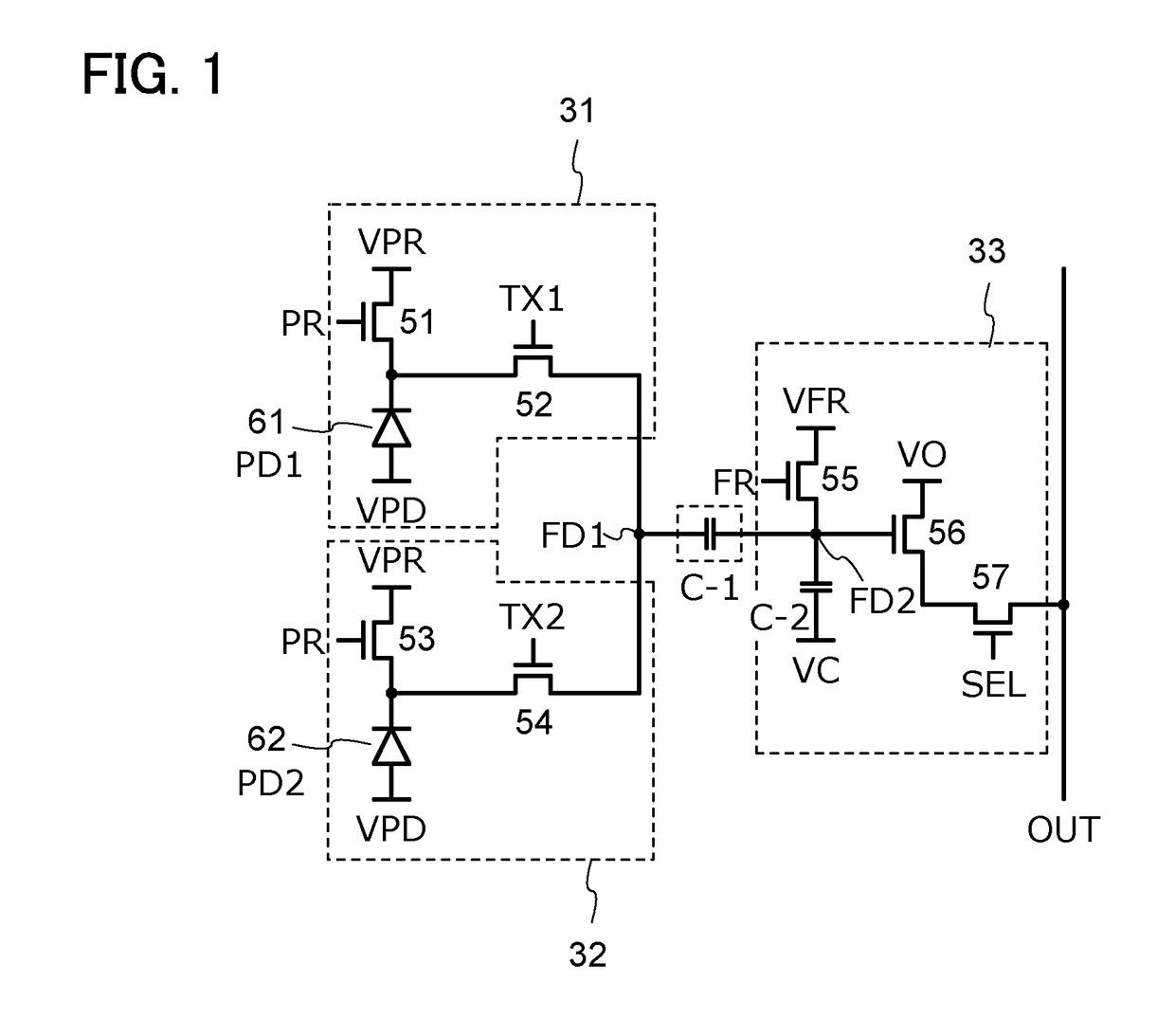
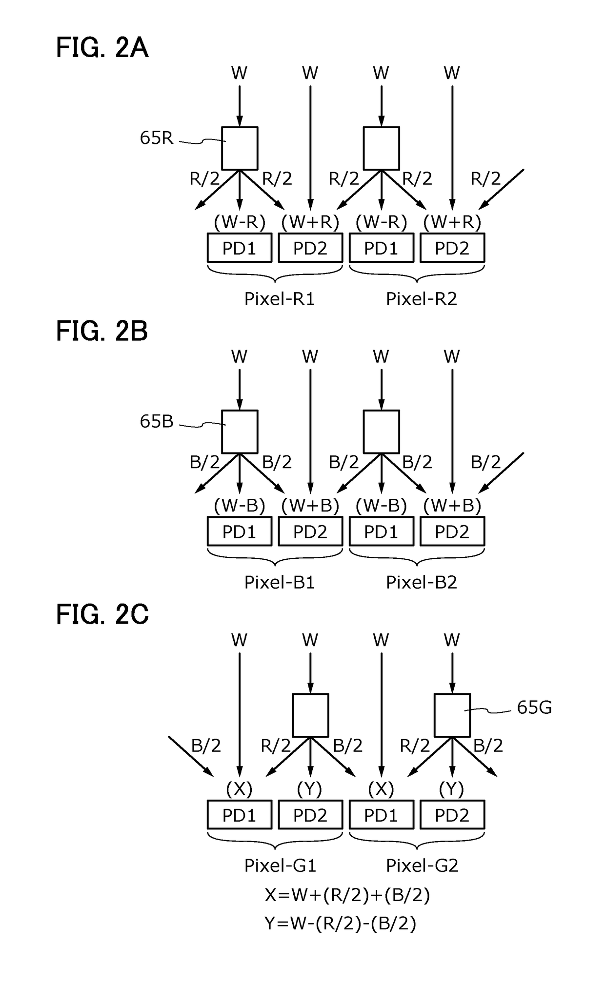
[0083]In the imaging device that is one embodiment of the present invention, a spectroscopic element can be used instead of a color filter. Therefore, loss of absorption by a color filter light can be suppressed, and the amount of light entering a photoelectric conversion element can be increased. In other words, the sensitivity of the imaging device can be increased.
[0084]Furthermore, a method of detecting a difference between signals obtained from two photoelectric conversion elements is used in order to extract imaging data of red (R), green (G), and blue (B) from dispersed light. In other words, arithmetic using an external circuit is not necessary, and thus the imaging device can have lower power consumption and operate at higher speed.
[0085]FIG. 1 is a circuit diagram of a pixel circuit that can be used for an imaging device of one embodiment of t...
embodiment 2
[0200]In this embodiment, an example of a driving method of a pixel circuit is described.
[0201]As described in Embodiment 1, the operation of the pixel circuit is repetition of the reset operation, the accumulation operation, and the selection operation. As imaging modes in which the whole pixel matrix is controlled, a global shutter system and a rolling shutter system are known.
[0202]FIG. 20 shows a timing chart in a global shutter system. Note that FIG. 20 shows, using an imaging device including a plurality of pixel circuits in matrix and including the circuits of FIG. 1 in the pixel circuits as an example, operations of the pixel circuits from the first row to the n-th row (n is a natural number of three or more).
[0203]In FIG. 20, a signal 501, a signal 502, and a signal 503 are signals input to the wirings PR connected to the pixel circuits in the first row, the second row, and the n-th row, respectively. Furthermore, a signal 504, a signal 506, and a signal 508 are signals inp...
embodiment 3
[0210]In this embodiment, a transistor including an oxide semiconductor that can be used in one embodiment of the present invention is described with reference to drawings. Note that in the drawings in this embodiment, some components are enlarged, reduced in size, or omitted for simplicity.
[0211]FIGS. 22(A) and (B) are a top view and a cross-sectional view illustrating a transistor 101 of one embodiment of the present invention. FIG. 22(A) is a top view, and a cross section in the direction of a dashed-dotted line B1-B2 in FIG. 22(A) corresponds to FIG. 22(B). A cross section in the direction of a dashed-dotted line B3-B4 in FIG. 22(A) corresponds to FIG. 28(A). In some cases, the direction of the dashed-dotted line B1-B2 is referred to as a channel length direction, and the direction of the dashed-dotted line B3-B4 is referred to as a channel width direction.
[0212]The transistor 101 includes an insulating layer 120 in contact with a substrate 115; an oxide semiconductor layer 130 ...
PUM
 Abstract
Description
Claims
Application Information
 - R&D
- Intellectual Property
- Life Sciences
- Materials
- Tech Scout
- Unparalleled Data Quality
- Higher Quality Content
- 60% Fewer Hallucinations
Browse by: Latest US Patents, China's latest patents, Technical Efficacy Thesaurus, Application Domain, Technology Topic, Popular Technical Reports.
© 2025 PatSnap. All rights reserved.Legal|Privacy policy|Modern Slavery Act Transparency Statement|Sitemap|About US| Contact US: help@patsnap.com


