Semiconductor device
- Summary
- Abstract
- Description
- Claims
- Application Information
AI Technical Summary
Benefits of technology
Problems solved by technology
Method used
Image

Examples
first embodiment
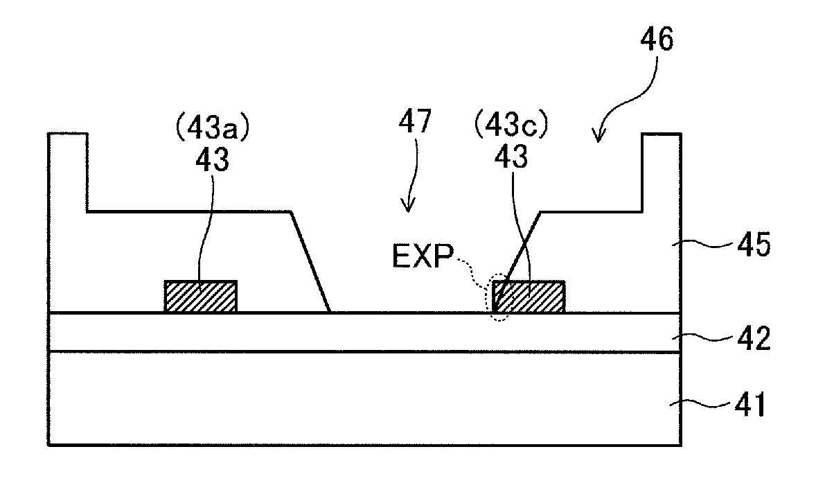
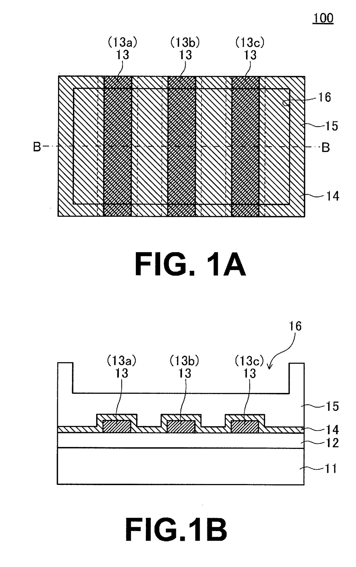
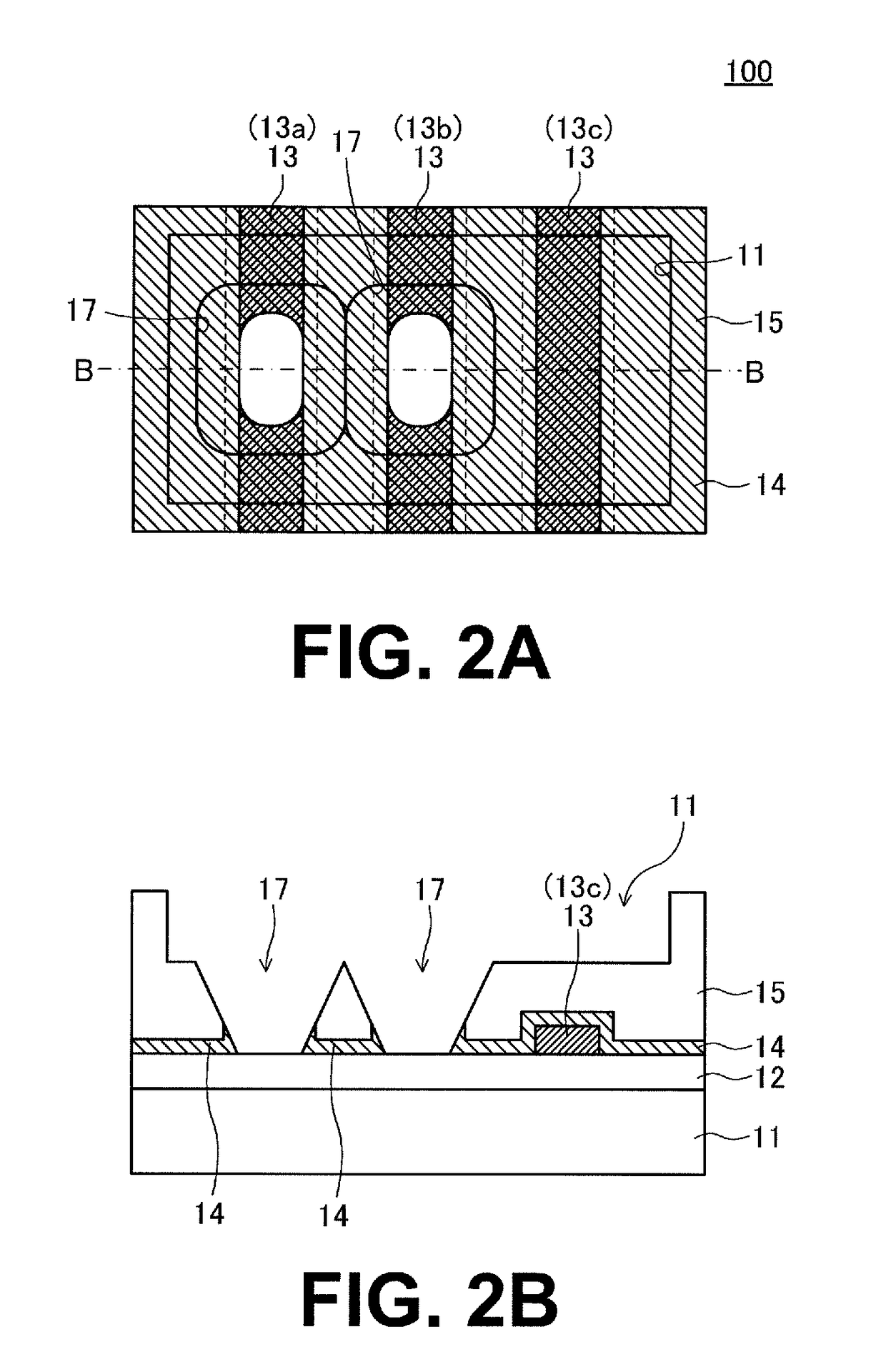
[0037]FIG. 1A and FIG. 1B are diagrams for illustrating the structure of a semiconductor device 100 according to a first embodiment of the present invention. FIG. 1A is a plan view of an area of the semiconductor device 100 that has a plurality of fuse elements formed therein. FIG. 1B is a sectional view taken along the line B-B of FIG. 1A.
[0038]As illustrated in FIG. 1A and FIG. 1B, the semiconductor device 100 of this embodiment includes an insulating film 12 formed on a semiconductor substrate 11, and a plurality of fuse elements 13 (13a, 13b, and 13c) formed on the insulating film 12 from a conductive body, e.g., a polysilicon film and arranged close to one another. A protective insulating film 14 is further formed to cover side surfaces and top surfaces of the plurality of fuse elements 13, and a top surface of the insulating film 12. An insulating film 15 is formed on the protective insulating film 14. A fuse opening 16 for laser irradiation is formed in the insulating film 15...
second embodiment
[0049]FIG. 3A and FIG. 3B are diagrams for illustrating the structure of a semiconductor device 200 according to the second embodiment. FIG. 3A is a plan view of an area of the semiconductor device 200 that has a plurality of fuse elements formed therein. FIG. 3B is a sectional view taken along the line B-B of FIG. 3A.
[0050]In the semiconductor device 200 of this embodiment, a protective insulating film 24 is formed on the left and right side surfaces of each fuse element 13 in place of the protective insulating film 14 in the semiconductor device 100 of the first embodiment which is illustrated in FIG. 1A and FIG. 1B. Similar to the protective insulating film 14, the protective insulating film 24 can be formed of an insulating film that is higher in mechanical strength than the insulating film 15, for example, a silicon nitride film or a silicon oxynitride film.
[0051]The rest of the configuration of the semiconductor device 200 is the same as the semiconductor device 100 of FIG. 1A...
third embodiment
[0059]FIG. 5A and FIG. 5B are diagrams for illustrating the structure of a semiconductor device 300 according to a third embodiment of the present invention. FIG. 5A is a plan view of an area of the semiconductor device 300 that has a plurality of fuse elements formed therein. FIG. 5B is a sectional view taken along the line B-B of FIG. 5A.
[0060]In the semiconductor device 300 of this embodiment, a protective insulating film 34 is formed in place of the protective insulating film 14 in the semiconductor device 100 of the first embodiment which is illustrated in FIG. 1A and FIG. 1B. Similar to the protective insulating film 14, the protective insulating film 34 can be formed of an insulating film that is higher in mechanical strength than the insulating film 15, for example, a silicon nitride film or a silicon oxynitride film.
[0061]The rest of the configuration of the semiconductor device 300 is the same as the semiconductor device 100 of FIG. 1A and FIG. 1B. Components of the semico...
PUM
 Abstract
Description
Claims
Application Information
 - R&D
- Intellectual Property
- Life Sciences
- Materials
- Tech Scout
- Unparalleled Data Quality
- Higher Quality Content
- 60% Fewer Hallucinations
Browse by: Latest US Patents, China's latest patents, Technical Efficacy Thesaurus, Application Domain, Technology Topic, Popular Technical Reports.
© 2025 PatSnap. All rights reserved.Legal|Privacy policy|Modern Slavery Act Transparency Statement|Sitemap|About US| Contact US: help@patsnap.com