Antenna device and electronic apparatus
- Summary
- Abstract
- Description
- Claims
- Application Information
AI Technical Summary
Benefits of technology
Problems solved by technology
Method used
Image

Examples
first preferred embodiment
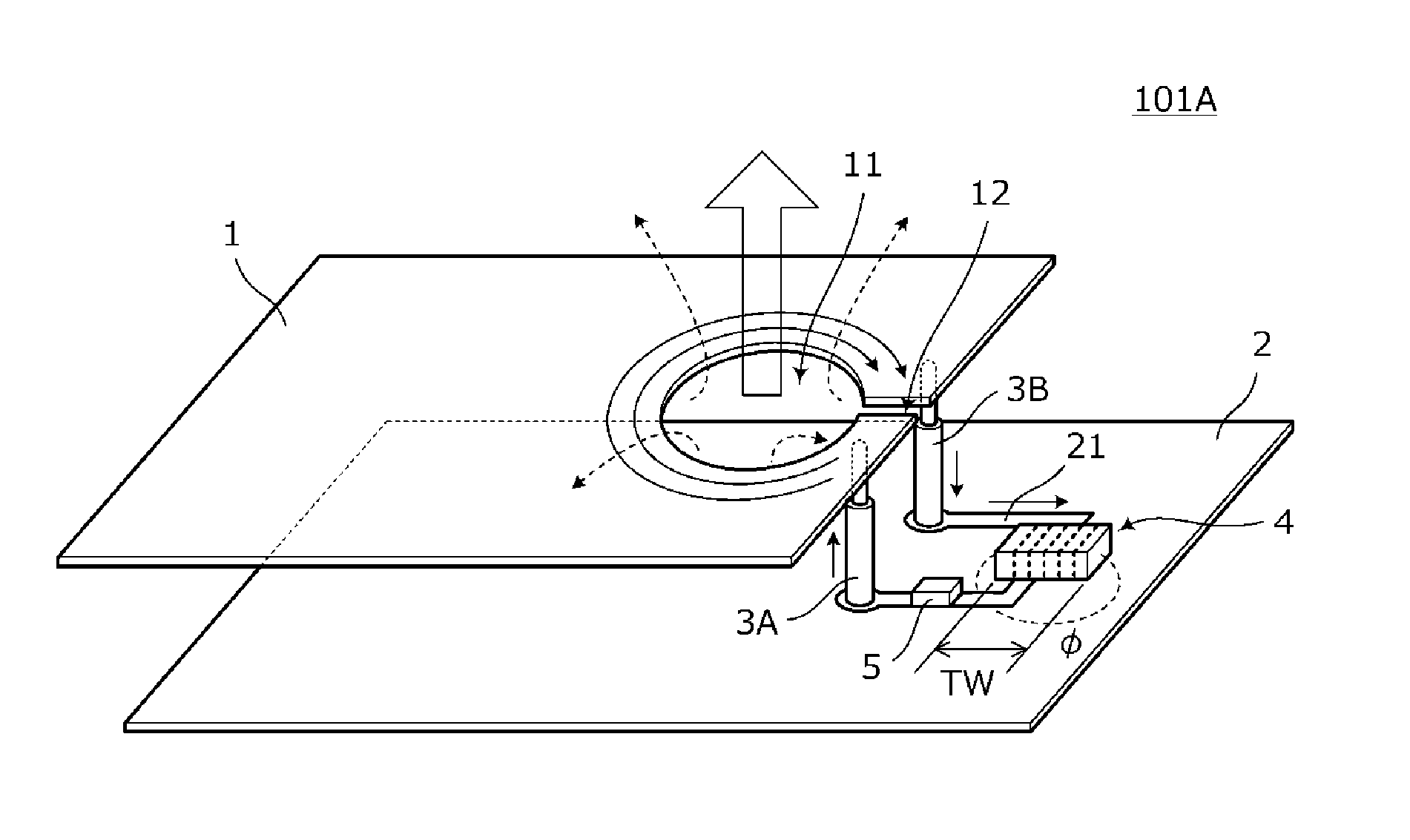
[0032]FIG. 1 is a perspective view of an antenna device 101A included in a portable electronic apparatus or the like according to a first preferred embodiment of the present invention. The antenna device 101 includes a conductive member 1 and a wiring substrate 2. A coupling line 21 that is conductive is disposed on the wiring substrate 2. The conductive member 1 and coupling line are electrically connected to each other with connecting conductors 3A and 3B interposed therebetween. One example of each of the connecting conductors 3A and 3B may be a spring pin.
[0033]A feeding coil 4 is magnetic-field coupled to the coupling line 21 and mounted on the wiring substrate 2. The wiring substrate 2 is connected to a chip capacitor 5 connected in series to the coupling line 21. In the present preferred embodiment, the capacitor connected to the coupling line 21 preferably is a chip capacitor, for example. It may be replaced with another type of capacitor, such as a lead capacitor.
[0034]The ...
second preferred embodiment
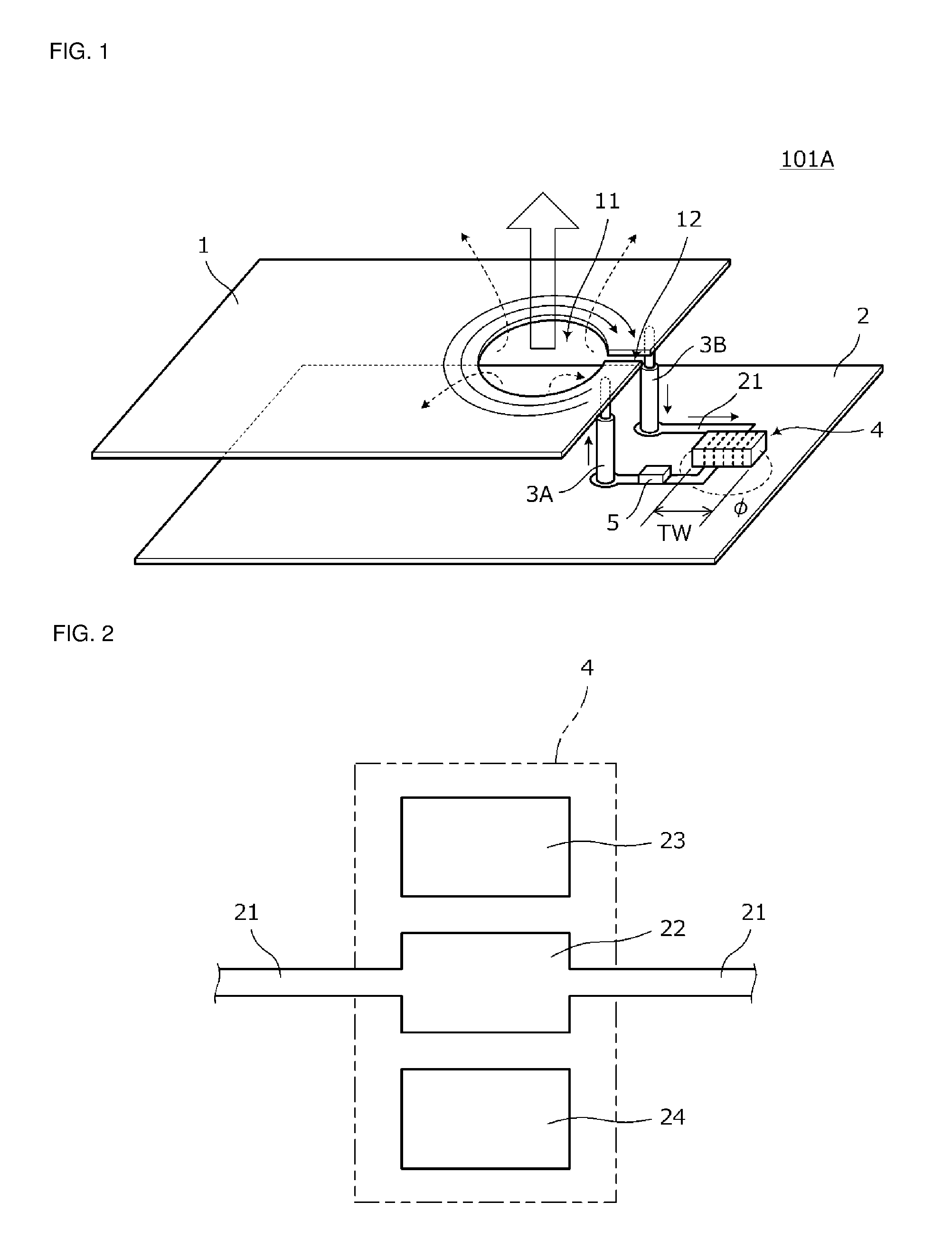
[0046]FIG. 7 is a perspective view of an antenna device 102A according to a second preferred embodiment of the present invention. The antenna device 102A includes a conductive member 1 and a wiring substrate 2. A coupling line 21 that is conductive is disposed on the wiring substrate 2. The conductive member 1 and coupling line are electrically connected to each other with connecting conductors 3A and 3B interposed therebetween. Two feeding coils 4A and 4B preferably are magnetic-field coupled to the coupling line 21 and mounted on the wiring substrate 2, for example. The wiring substrate 2 is connected to a chip capacitor 5 connected in series to the coupling line 21.
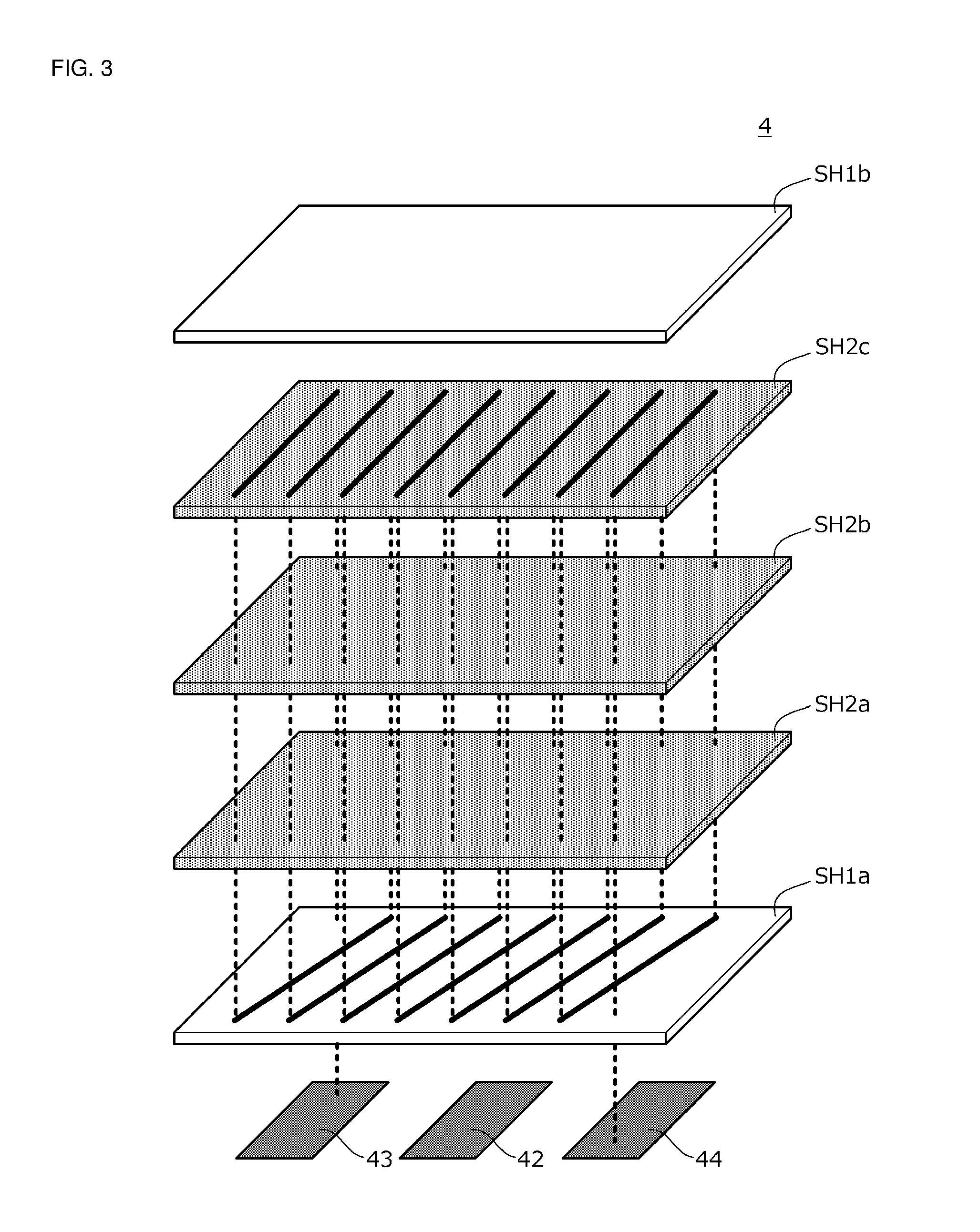
[0047]The configuration of each of the feeding coils 4A and 4B is shown in FIG. 3. The two feeding coils 4A and 4B are connected in series or parallel to each other and are connected to the feeder circuit.
[0048]In accordance with a preferred embodiment of the present invention, an antenna device can include three or mo...
third preferred embodiment
[0052]FIG. 9 is a perspective view of an antenna device 103 according to a third preferred embodiment of the present invention. The antenna device 103 includes a conductive member 1 and a wiring substrate 2. A coupling line 21 that is conductive is disposed on the wiring substrate 2. The conductive member 1 and coupling line are electrically connected to each other with connecting conductors 3A and 3B interposed therebetween. A feeding coil 4 is magnetic-field coupled to the coupling line 21 and mounted on the wiring substrate 2. The wiring substrate 2 is connected to a chip capacitor 5 connected in series to the coupling line 21.
[0053]Ground patterns 26 are disposed on the wiring substrate 2. Chip capacitors 6A and 6B are disposed between the ground patterns 26 and coupling line 21. The ground patterns 26 are preferably in a vicinity of or adjacent to the locations where the connecting conductors 3A and 3B and coupling line 21 are connected.
[0054]The chip capacitors 6A and 6B prefe...
PUM
 Abstract
Description
Claims
Application Information
 - R&D
- Intellectual Property
- Life Sciences
- Materials
- Tech Scout
- Unparalleled Data Quality
- Higher Quality Content
- 60% Fewer Hallucinations
Browse by: Latest US Patents, China's latest patents, Technical Efficacy Thesaurus, Application Domain, Technology Topic, Popular Technical Reports.
© 2025 PatSnap. All rights reserved.Legal|Privacy policy|Modern Slavery Act Transparency Statement|Sitemap|About US| Contact US: help@patsnap.com