
Formation of boron-doped titanium metal films with high work function

a metal film, high work function technology, applied in the direction of basic electric elements, electrical apparatus, semiconductor devices, etc., can solve the problems of undesirable pmos metal gate application, plasma treatment discouraged,

Active Publication Date: 2017-01-26
ASM IP HLDG BV
View PDF4 Cites 311 Cited by
  • Summary
  • Abstract
  • Description
  • Claims
  • Application Information

AI Technical Summary

Benefits of technology

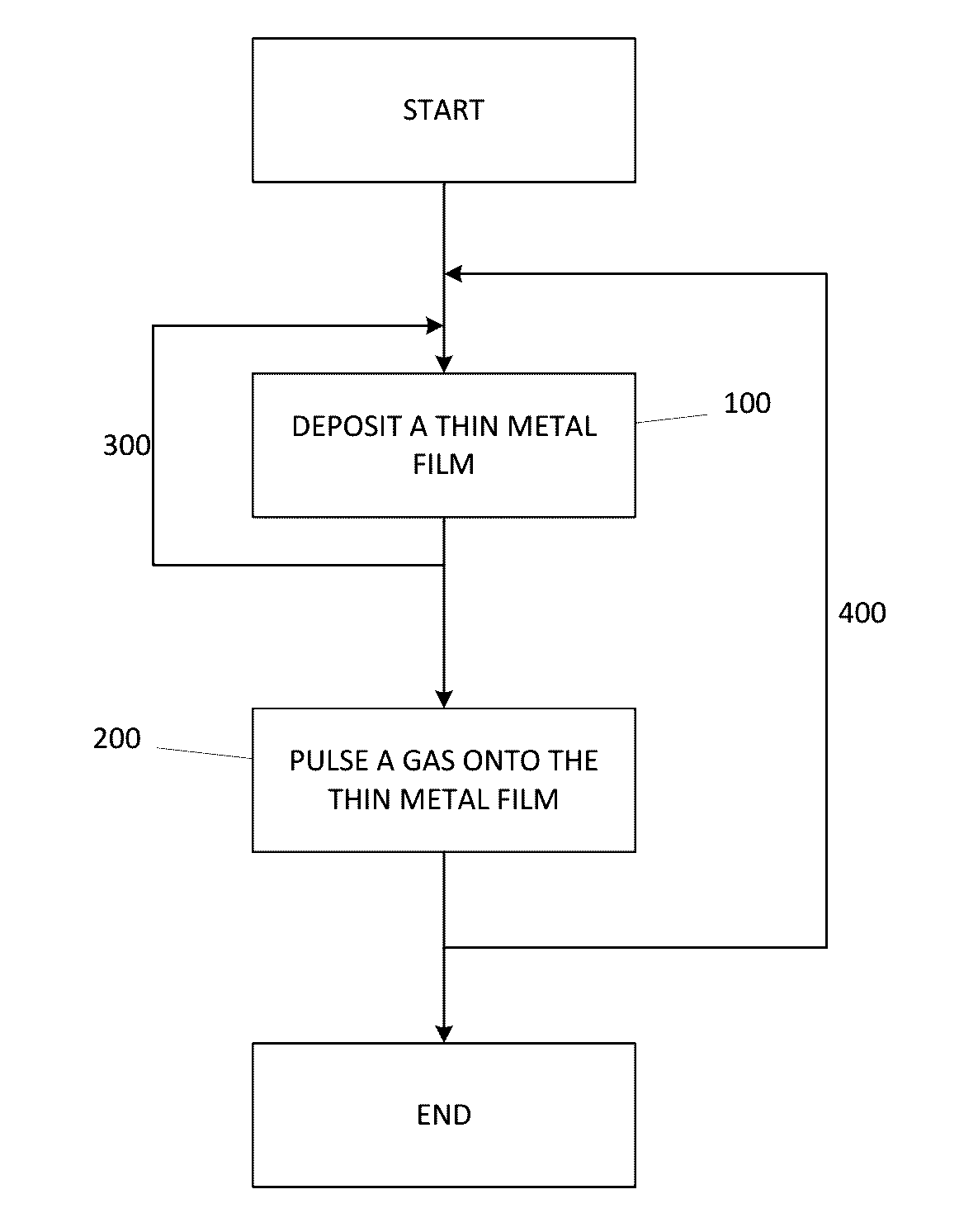
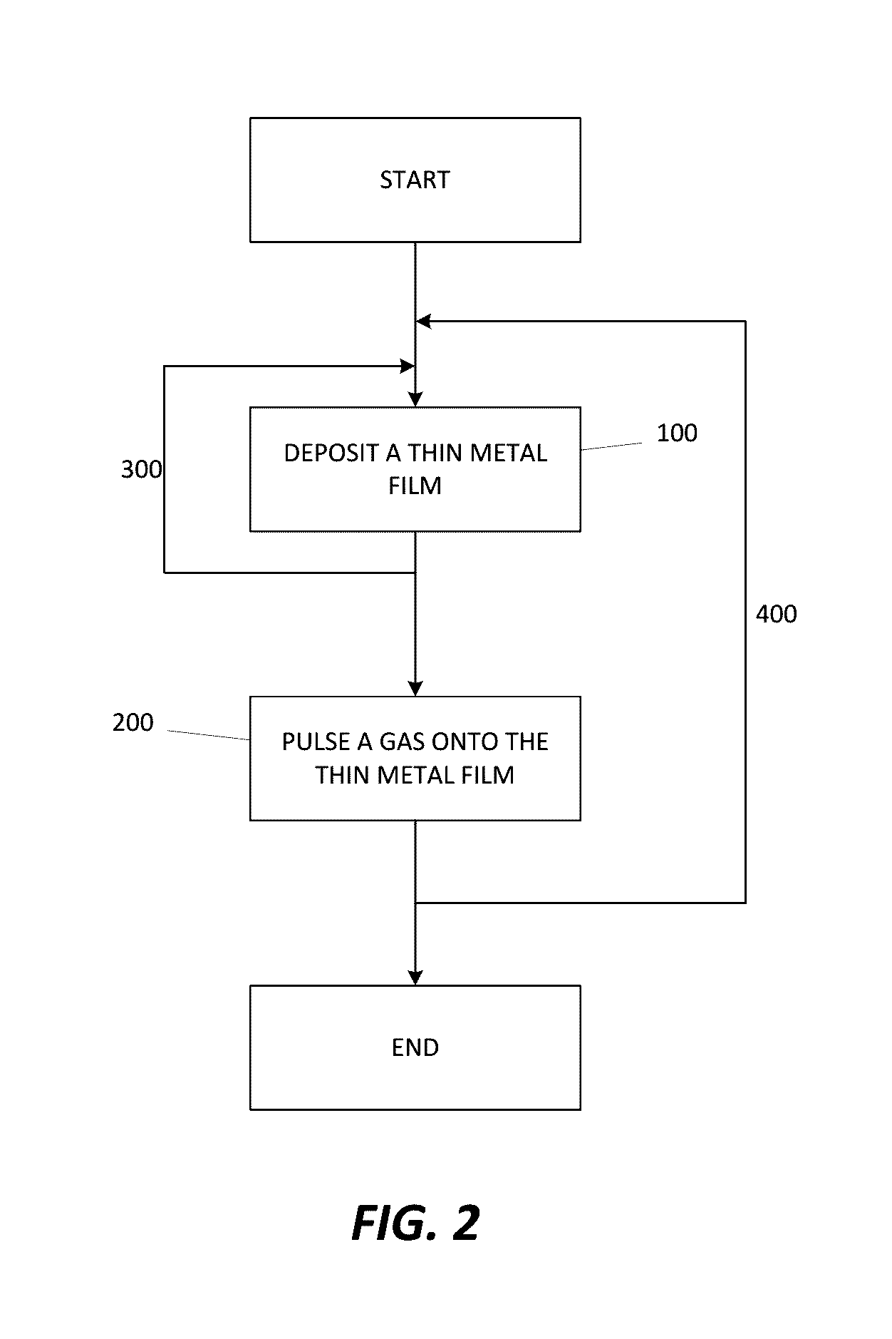
The patent describes a method for creating a metallic film on a semiconductor device by depositing a thin layer of metal and then pulsing it with a gas. The method involves a series of steps, including purging the device with inert gas and pulsing it with a nitridizing gas. The invention is not limited to the specific embodiments described and other embodiments can be developed based on the teachings of the patent. The technical effect of the invention is to provide a reliable and effective method for creating metallic films on semiconductor devices, which can be useful in various applications.

Problems solved by technology

While the TiN films created through the plasma or PEALD treatment have exhibited higher electronic work functions, plasma treatments have been discouraged for pMOS metal gate applications due to concerns over plasma damage.
A greater EOT is undesirable because it leads to a reduced capacitance.

Method used


Image

  • Formation of boron-doped titanium metal films with high work function
  • Formation of boron-doped titanium metal films with high work function
  • Formation of boron-doped titanium metal films with high work function

Examples


Embodiment Construction

[0015]Although certain embodiments and examples are disclosed below, it will be understood by those in the art that the invention extends beyond the specifically disclosed embodiments and / or uses of the invention and obvious modifications and equivalents thereof. Thus, it is intended that the scope of the invention disclosed should not be limited by the particular disclosed embodiments described below.

[0016]Embodiments of the current invention relate to the doping of Boron into titanium metal films, such as Titanium Nitride (“TiN”). The result is a Boron-doped metal film, such as Titanium Boron Nitride. The doping of Boron into the formation of TiN films has shown promise as a result of Boron's ability to remove excess chlorine in the film resulting from the passing of Titanium Chloride (“TiCl4”) gas. For example, Diborane in gaseous form reacts with the Chlorine in the film with the following reaction.

B2H6 (g)+6Cl (in-film)→2BCl3 (g)+3H2 (g)

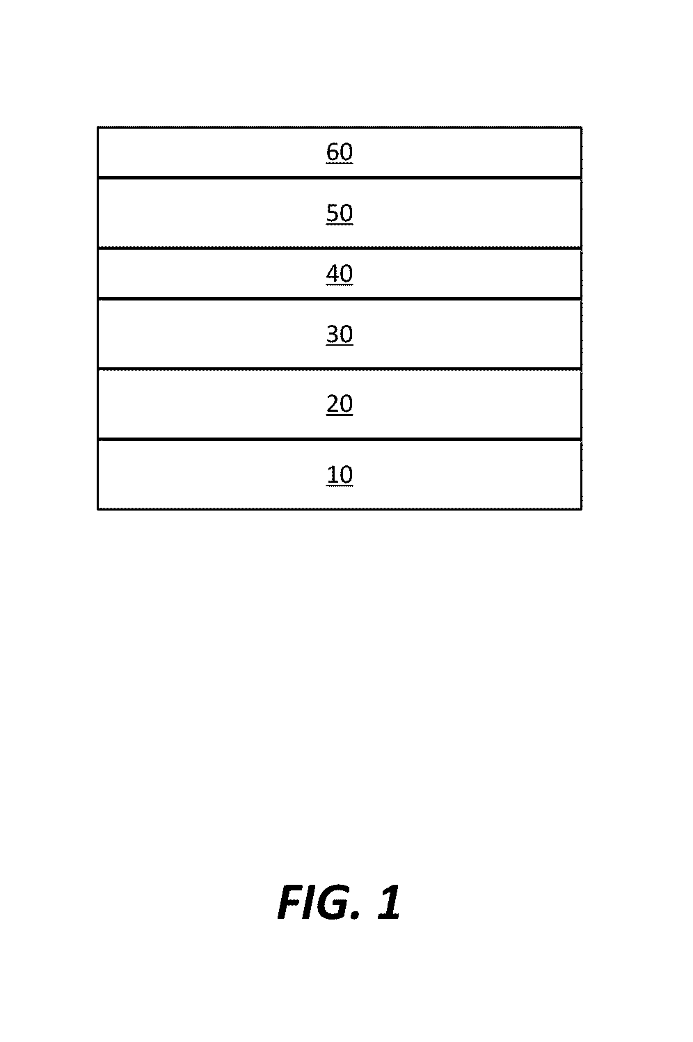
[0017]FIG. 1 illustrates a device made in...


PUM

PropertyMeasurementUnit
thicknessaaaaaaaaaa
thicknessaaaaaaaaaa
thicknessaaaaaaaaaa

Abstract

A method for forming a Boron doped metallic film, such as Titanium Boron Nitride, is disclosed. The method allows for creation of the metallic film with a high work function and low resistivity, while limiting the increase in effective oxide thickness. The method comprises a thin metallic layer deposition step as well as a Boron-based gas pulse step. The Boron-based gas pulse deposits Boron and allows for the removal of excess halogens within the metallic film. The steps may be repeated in order to achieve a desired thickness of the metallic film.

Description

FIELD OF INVENTION[0001]The present disclosure generally relates to formation of a metallic film. In particular, the present disclosure relates to a method for forming a metallic film with a high electronic work function (“eWF”).BACKGROUND OF THE DISCLOSURE[0002]In applications such as the formation of pMOS metal gates, it is generally desirable to deposit a metal with a high work function and a low resistivity. A high work function allows for a lower threshold voltage offset and a lower off current. From this, a lower leakage current can be achieved and a threshold voltage swing can be improved. A low resistivity positively affects a cycle time and allows for higher speed processing.[0003]Formation of Titanium Nitride (“TiN”) films has been achieved using different methods. However, the TiN films created have exhibited different work functions based on the method used. For example, TiN films created through Atomic Layer Deposition (“ALD”) have demonstrated work functions ranging be...

Claims


Application Information

Patent Timeline
Patent Type & Authority Applications(United States)
IPC IPC(8): H01L21/285
CPCH01L21/28562H01L21/32051H01L21/28088H01L21/28194H01L21/28211H01L21/0228H01L21/02046H01L2924/01005H01L2924/01022H01L21/28202
Inventor MILLIGAN, ROBERT BRENNAN
Owner ASM IP HLDG BV
Learn More