Stacked package device and method for fabricating the same

a technology of stacked package and packaging device, which is applied in the direction of semiconductor devices, basic electric elements, electrical equipment, etc., can solve the problems of reducing the overall reliability of the stacked package device, metal wires are easily oxidized, and the functionality of the semiconductor chip to be increased and become more complex

Active Publication Date: 2016-11-10
WINBOND ELECTRONICS CORP
View PDF1 Cites 6 Cited by
  • Summary
  • Abstract
  • Description
  • Claims
  • Application Information

AI Technical Summary

Benefits of technology

The patent text discusses the challenges faced in fabricating stacked package devices, due to the easy oxidation of metal wires and the increasing complexity of chip design. The technical effect of the patent is to provide a method for addressing these challenges and improving the reliability of stacked package devices.

Problems solved by technology

As demand increases for electronic products such as digital cameras, camera phones, and displays, semiconductor technology for products made therefrom must develop rapidly, especially as product trends show an increased requirement for the semiconductor chip size to be miniaturized, and for the functionality of the semiconductor chip to be increased and become more complex.
However, metal wires are easily oxidized because they are exposed to the external environment before the encapsulation molding process is performed.
Moreover, as the semiconductor chip size is to be miniaturized, and the complexity of the design of the semiconductor chip is to be increased, problems may arise with the shifting, bridging and / or breakage of metal wires due to the molding compound used during the encapsulation molding process, and this results in a reduction of the overall reliability of the stacked package device.

Method used


Image

  • Stacked package device and method for fabricating the same
  • Stacked package device and method for fabricating the same
  • Stacked package device and method for fabricating the same

Examples


Embodiment Construction

[0014]The following description is of the best-contemplated mode of carrying out the disclosure. This description is made for the purpose of illustrating the general principles of the disclosure and should not be taken in a limiting sense. These are, of course, merely examples and are not intended to be limited. In addition, the disclosure may repeat reference numerals and / or letters in the various examples. This repetition is for the purpose of simplicity and clarity and does not in itself dictate a relationship between the various embodiments and / or configurations discussed.

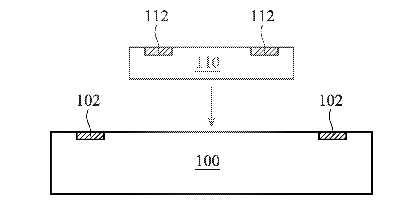
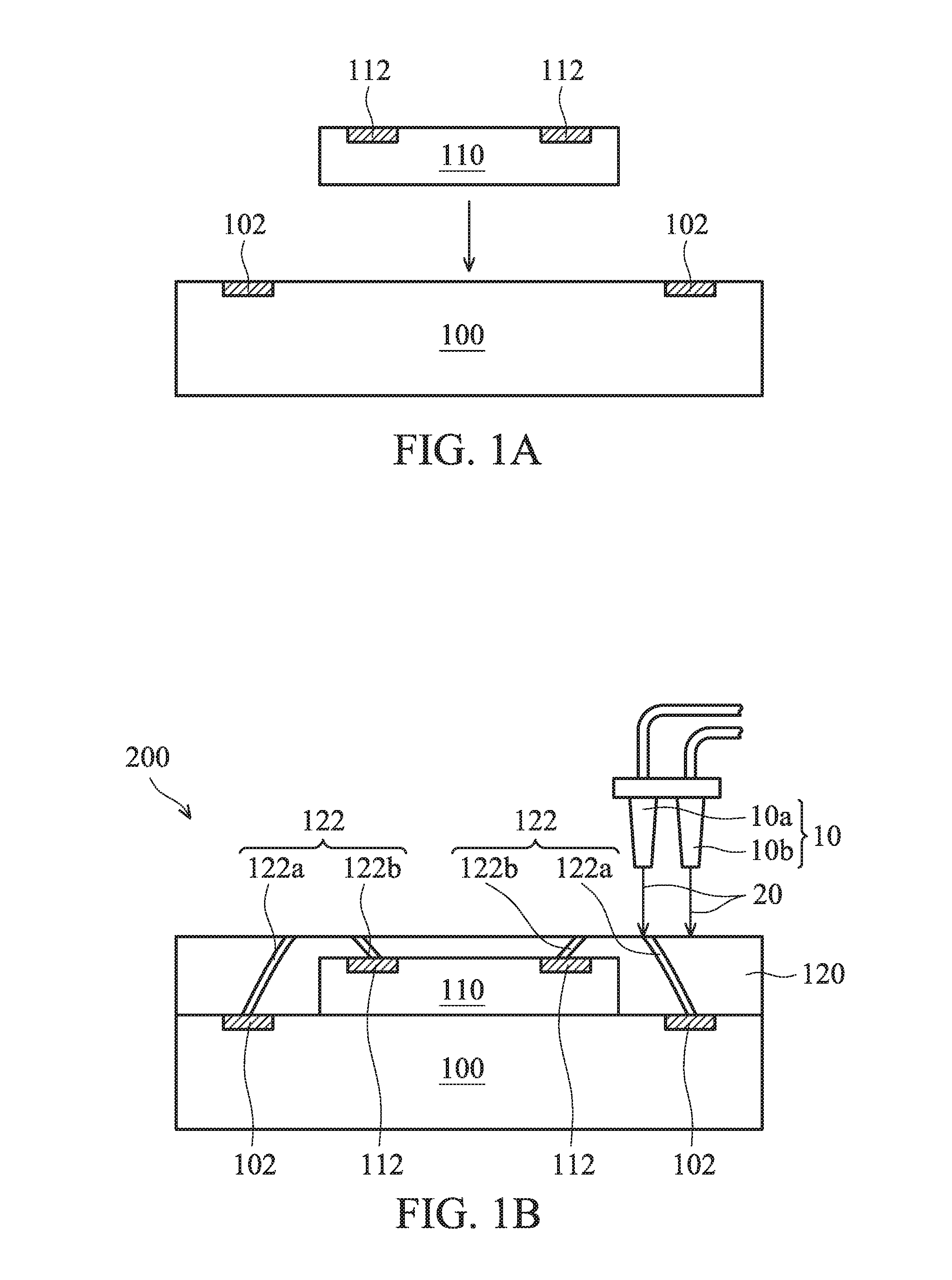
[0015]FIG. 1B illustrates a cross section of an exemplary embodiment of a stacked package device according to the present disclosure. In the embodiment, the stacked package device 200 includes a first substrate 100, a second substrate 110, an encapsulating layer 120 and a plurality of bonding wires 122. In one embodiment, the first substrate 100 may include a PCB, a wafer, a chip, or a combination thereof. More...


PUM


Abstract

A method for fabricating a stacked package device is provided. A second substrate is adhered onto a first substrate. The first substrate includes a plurality of first bonding pads, and the second substrate includes a plurality of second bonding pads. A three-dimensional (3D) printing is performed to form an encapsulating layer covering the first substrate and the second substrate and to form a plurality of bonding wires in the encapsulating layer. Each bonding wire includes a first portion connected to one of the plurality of first bonding pads. The disclosure also provides a stacked package device formed by such a method.

Description

CROSS REFERENCE TO RELATED APPLICATIONS[0001]This application claims the benefit of China Patent Application No. 201510230568.7 filed on May 8, 2015, entitled “STACKED PACKAGE DEVICE AND METHOD FOR FABRICATING THE SAME” which is hereby incorporated herein by reference.BACKGROUND[0002]1. Field of the Disclosure[0003]The present disclosure relates to a semiconductor technology, and in particular, it relates to a stacked package device fabricated by using a three-dimensional (3D) printing technology.[0004]2. Description of the Related Art[0005]As demand increases for electronic products such as digital cameras, camera phones, and displays, semiconductor technology for products made therefrom must develop rapidly, especially as product trends show an increased requirement for the semiconductor chip size to be miniaturized, and for the functionality of the semiconductor chip to be increased and become more complex.[0006]Typically, a semiconductor chip includes an integrated circuit inclu...

Claims


Application Information

Patent Timeline
IPC IPC(8): H01L25/065H01L25/00
CPCH01L25/0657H01L2225/06582H01L2225/06506H01L25/50H01L2924/181H01L2224/48091H01L2924/00012H01L2924/00014
Inventor CHIAO, YU-CHENGCHAN, TUNG-YILIN, CHEN-HSIHO, CHIA HUACHAN, MENG-CHANGCHOU, HSIN-HUNG
Owner WINBOND ELECTRONICS CORP
Why Eureka
Try Eureka