Novel Methods of Preparing Nanodevices

a technology of nano-electromechanical devices and nano-electromechanical devices, which is applied in the field of new methods of preparing nano-electromechanical devices, can solve the problems of high variability in device quality and commercial application of nano-electromechanical devices

Inactive Publication Date: 2016-10-20
UNIV OF COLORADO THE REGENTS OF +1
View PDF2 Cites 6 Cited by
  • Summary
  • Abstract
  • Description
  • Claims
  • Application Information

AI Technical Summary

Benefits of technology

The invention provides methods of preparing nanodevices by coating a solid supporting material layer with a thin solid material layer using atomic layer deposition (ALD) and patterning it using etching or other techniques. The invention also provides nanodevices prepared using these methods. The methods and devices can be used for various applications such as bolometers, transducers, temperature sensors, and more. The invention provides improved methods for preparing nanodevices with ALD-generated layers.

Problems solved by technology

Key problems preventing the commercial application of nano-electromechanical devices have included low-yields and high device quality variability.

Method used


Image

  • Novel Methods of Preparing Nanodevices
  • Novel Methods of Preparing Nanodevices
  • Novel Methods of Preparing Nanodevices

Examples


example 1

Electrical Layer Processing

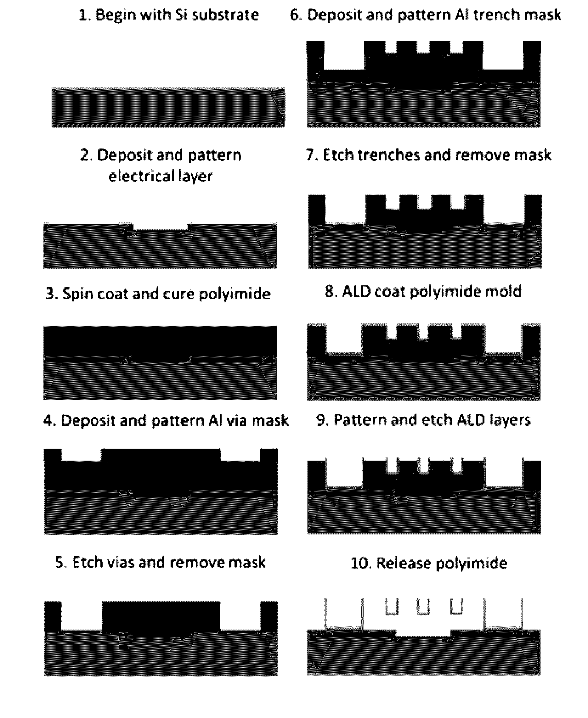
[0106]The electrical layer was formed via lift-off patterning with negative photoresist. After pattern exposure and development, an aluminum film nominally 100 nm in thickness was evaporated, followed by lift-off performed using an ultrasonic bath.

Polyimide Processing

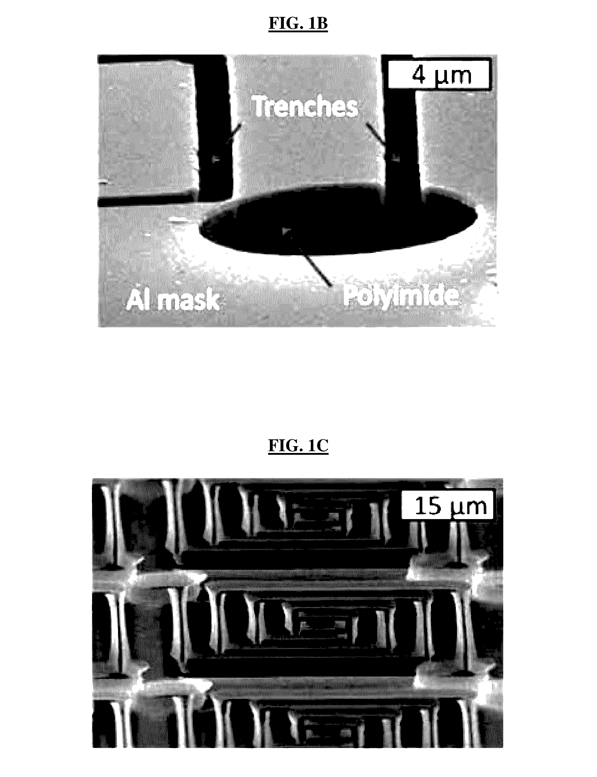
[0107]An adhesion promotion chemical was applied to the substrate and polyimide was spun onto the adhesion layer. The resultant structure was then cured at elevated temperatures. In non-limiting embodiments, thicknesses of the structure using the process were typically from about 2.5 μm to about 4.5 μm. Vias and trenches were both etched utilizing a thermally evaporated 100-nm aluminum mask, which was patterned using negative photoresist and lift-off processing. The etch was done using anisotropic reactive ion etching (RIE) with O2 plasma. The aluminum mask was removed in etchant.


PUM

PropertyMeasurementUnit
Thicknessaaaaaaaaaa
Thicknessaaaaaaaaaa
Heat capacityaaaaaaaaaa

Abstract

The present invention relates to novel nano- and micro-electromechanical devices and novel methods of preparing them. In one aspect, the invention includes methods of preparing a nanodevice. In certain embodiments, the methods comprise coating a polymer layer with a first at least one thin solid material layer using atomic layer deposition (ALD), thus forming an ALD-generated layer. In other embodiments, the methods comprise patterning the first at least one thin solid material layer to form a nanodevice. In yet other embodiments, the methods comprise releasing the nanodevice from the polymer layer.

Description

CROSS-REFERENCE TO RELATED APPLICATIONS[0001]The present application claims priority under 35 U.S.C. §119(e) to U.S. Provisional Patent Application No. 61 / 931,292, filed Jan. 24, 2014, which is incorporated herein by reference in its entirety.STATEMENT REGARDING FEDERALLY SPONSORED RESEARCH OR DEVELOPMENT[0002]This invention was made with government support under grant number N66001-10-1-4007 awarded by DOD / DARPA. The government has certain rights in the invention.BACKGROUND OF THE INVENTION[0003]There has been great interest in identifying novel methods of preparing nano- and micro-electromechanical devices.[0004]Micro-electromechanical systems (MEMS) devices comprise components between about 1 to 100 μm in size (i.e., 0.001 to 0.1 mm), and MEMS devices generally range in size from 20 μm to 1.0 mm. Such devices may be prepared using modified semiconductor device fabrication technologies, which are commonly used to make electronics. Patterning of the device is usually achieved using...

Claims


Application Information

Patent Timeline
IPC IPC(8): B82B3/00C23C16/01C23C16/455B82B1/00C23C16/14C23C16/02B05D7/24B05D3/14C23C16/56C23C16/40
CPCB82B3/008C23C16/56C23C16/01C23C16/45555C23C16/45525C23C16/45553C23C16/14C23C16/0245B05D7/24B05D3/145B82B1/005C23C16/403B82Y30/00B81C1/0019B81C1/00492H01L2924/0002H01L2924/00
Inventor BRIGHT, VICTOR M.GEORGE, STEVENBROWN, JOSEPH J.EIGENFELD, NATHAN T.GRAY, JASON M.SKIDMORE, GEORGE DEE
Owner UNIV OF COLORADO THE REGENTS OF
Why Eureka
Try Eureka