Optical device
- Summary
- Abstract
- Description
- Claims
- Application Information
AI Technical Summary
Benefits of technology
Problems solved by technology
Method used
Image

Examples
Embodiment Construction
[0033]Reference will now be made in detail to the present preferred embodiments of the invention, examples of which are illustrated in the accompanying drawings. Wherever possible, the same reference numbers are used in the drawings and the description to refer to the same or like parts.
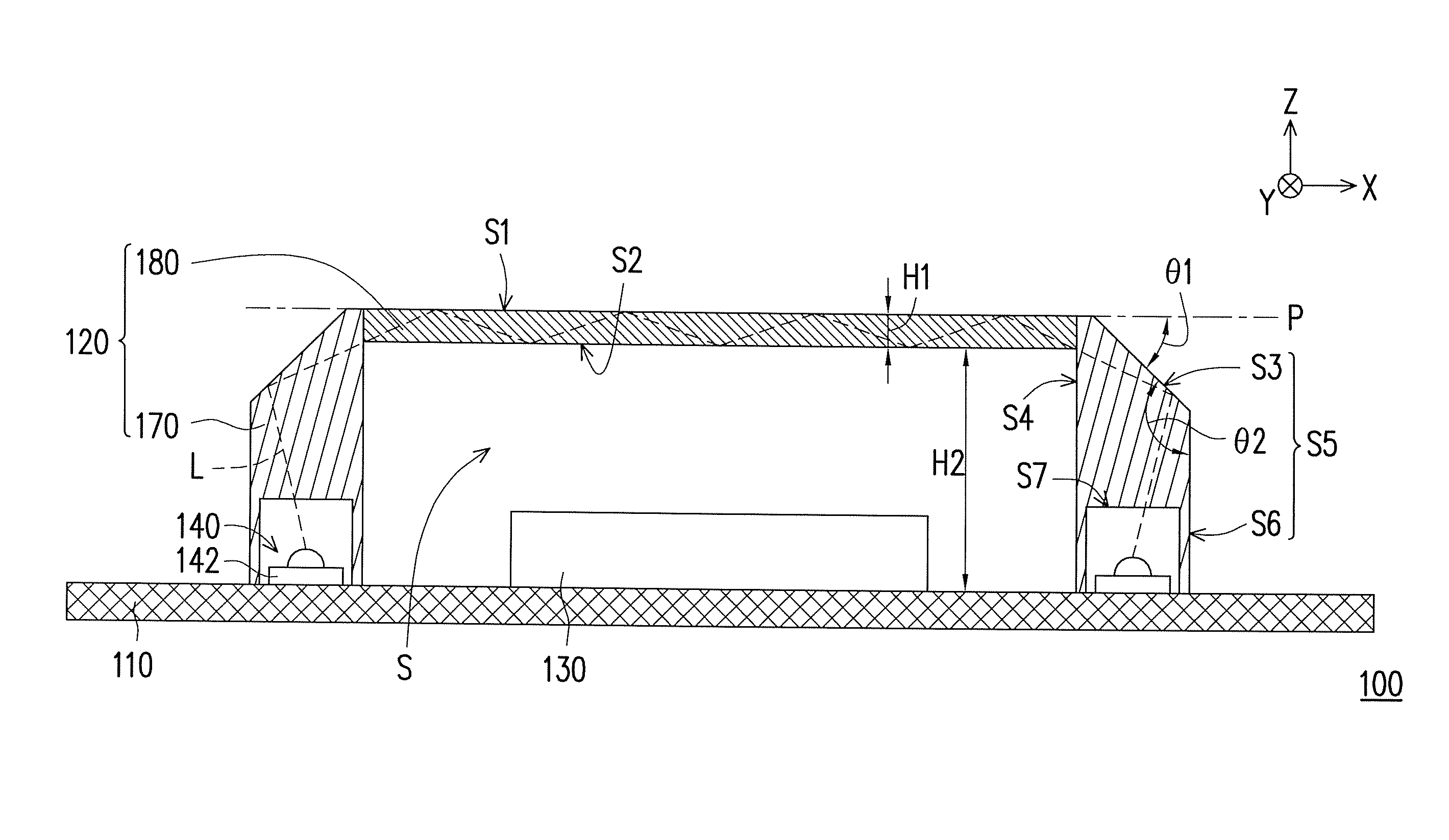
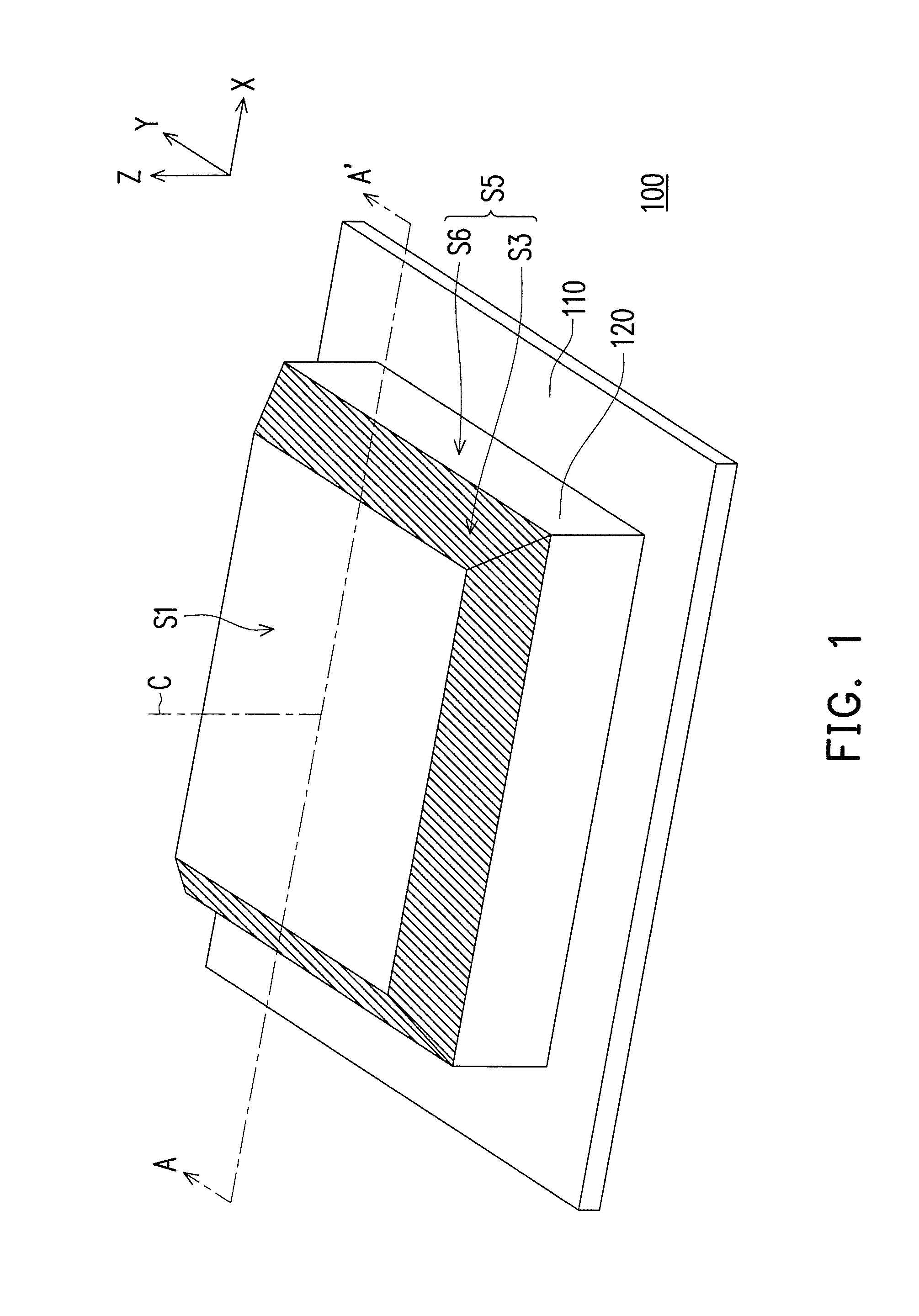
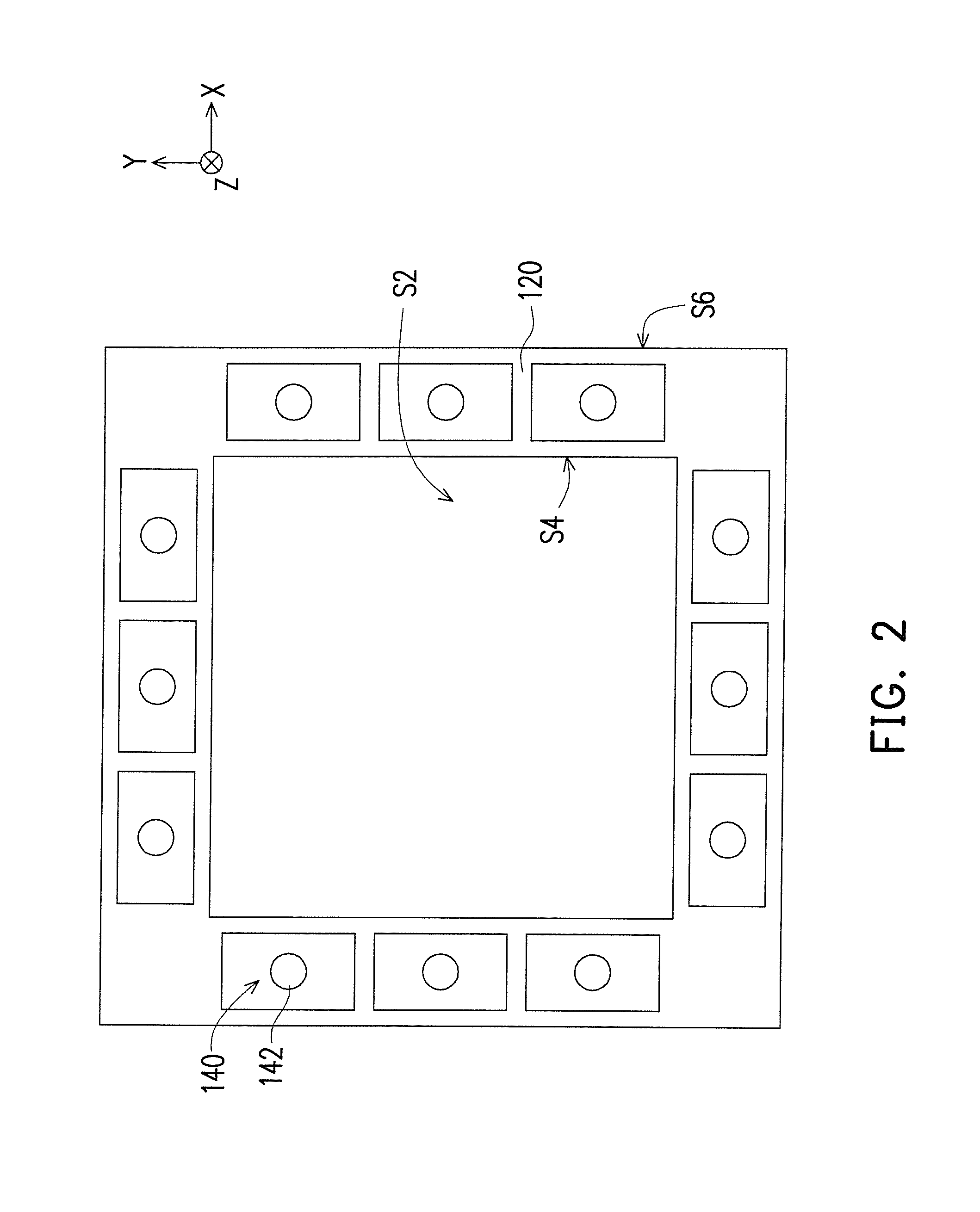
[0034]FIG. 1 is a three-dimensional schematic view of an optical device according to an embodiment of the invention. FIG. 2 is a bottom view of the optical device of FIG. 1. FIG. 3 is a schematic cross-sectional view of the optical device of FIG. 1 taken along the line A-A′. FIG. 4 is the schematic cross-sectional view of the optical device of FIG. 3 contacting a finger. Referring to FIG. 1 to FIG. 4, an optical device 100 includes an image capture unit 130, at least one light emitting device 142, and a light conductor 120. The light conductor 120 defines a space S above a substrate 110 on which the image capture unit 130 is disposed. The light conductor 120 includes a central portion 180 and a surro...
PUM
 Abstract
Description
Claims
Application Information
 - R&D
- Intellectual Property
- Life Sciences
- Materials
- Tech Scout
- Unparalleled Data Quality
- Higher Quality Content
- 60% Fewer Hallucinations
Browse by: Latest US Patents, China's latest patents, Technical Efficacy Thesaurus, Application Domain, Technology Topic, Popular Technical Reports.
© 2025 PatSnap. All rights reserved.Legal|Privacy policy|Modern Slavery Act Transparency Statement|Sitemap|About US| Contact US: help@patsnap.com