
Independent power collapse methodology

Active Publication Date: 2016-08-18
QUALCOMM INC
View PDF13 Cites 36 Cited by
  • Summary
  • Abstract
  • Description
  • Claims
  • Application Information

AI Technical Summary

Benefits of technology

The disclosed principles allow for efficient and organized isolation and de-isolation of power domains in a modular way. This promotes processing nodes or logic within each power domain to operate autonomously, leading to better power efficiency, reliability, and modular system design. The decoupling of decisions between power domain isolation and power collapse reduces design complexity and allows for increased flexibility in power control. Additionally, isolation is transparent to processing nodes, reducing the processing overhead associated with power domain isolation and power collapse.

Problems solved by technology

In many electrical devices, and especially mobile devices, power consumption of the associated integrated circuits is a major design consideration.
This power consumption primarily comprises switching current that results from actively functioning circuitry and leakage current that results from inactive circuitry passively drawing power.
But, the lower threshold voltages and smaller-size transistors can also lead to higher leakage currents, where “leakage” currents are, e.g., currents passing through transistors that are in an “off” state.
Such leakage currents generally become more problematic as integrated circuit transistors continue to scale down in size.

Method used


Image

  • Independent power collapse methodology
  • Independent power collapse methodology
  • Independent power collapse methodology

Examples


Embodiment Construction

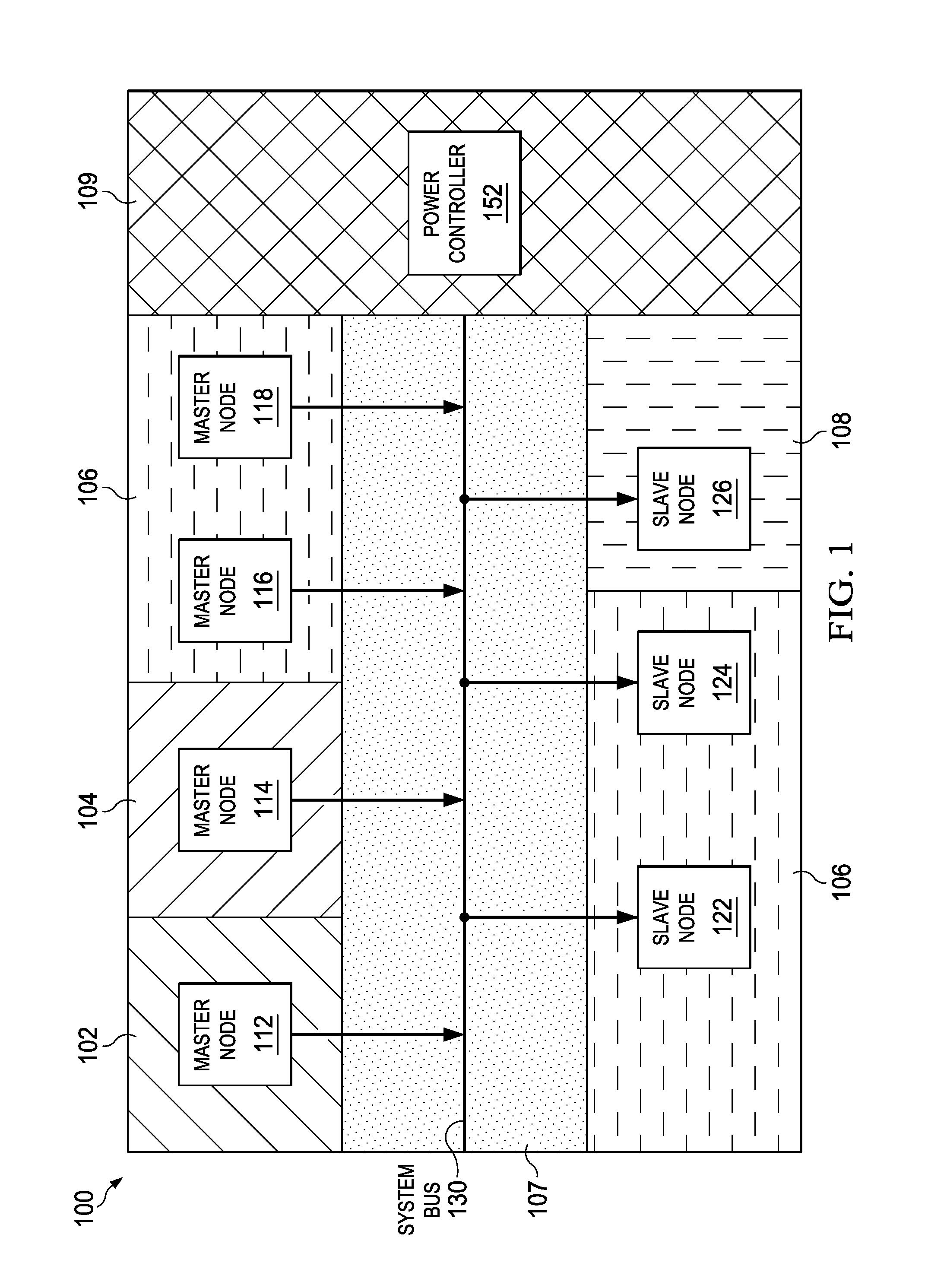
[0027]FIG. 1 shows a block diagram of a system 100 having a plurality of power domains that may be implemented within an integrated circuit. The system comprises a plurality of master nodes 112, 114, 116, 118 and a plurality of slave nodes 122, 124, 126. The master nodes may communicate with the slave nodes and with each other via a system bus 130. A master node may generally initiate commands and requests on the system bus 130, whereas a slave node may generally receive commands and requests on the system bus 130. For example, the primary processing core or cores of a device (e.g., a digital signal processing core) may serve as master nodes, whereas memory devices and peripheral units (e.g., providing USB or Bluetooth connectivity) may serve as slave nodes. The choices of master nodes and slave nodes depend on the desired topology of the end system.

[0028]The master nodes 112, 114, 116, 118, the slave nodes 122, 124, 126, and the system bus 130 may be implemented in a plurality of p...


PUM


Abstract

The feature size of semiconductor devices continues to decrease in each new generation. Smaller channel lengths lead to increased leakage currents. To reduce leakage current, some power domains within a device may be powered off (e.g., power collapsed) during periods of inactivity. However, when power is returned to the collapsed domains, circuitry in other power domains may experience significant processing overhead associated with reconfiguring communication channels to the newly powered domains. Provided in the present disclosure are exemplary techniques for isolating power domains to promote flexible power collapse while better managing the processing overhead associated with reestablishing data connections.

Description

BACKGROUND[0001]1. Field of the Disclosure[0002]The present application generally relates to power efficient semiconductor design and, more specifically, to systems and methods for isolating power domains within integrated circuits.[0003]2. Description of Related Art[0004]In many electrical devices, and especially mobile devices, power consumption of the associated integrated circuits is a major design consideration. This power consumption primarily comprises switching current that results from actively functioning circuitry and leakage current that results from inactive circuitry passively drawing power.[0005]As integrated circuit fabrication technology continually improves and migrates to smaller geometry, the size of transistors (e.g., their minimum channel length) continues to shrink. Additionally, the threshold voltage for smaller-size transistors, which is the voltage at which a transistor turns on, is often reduced to improve operating speed. The lower threshold voltages perm...

Claims


Application Information

Patent Timeline
IPC IPC(8): G06F1/26
CPCG06F1/26G06F1/3237H03K19/0016G06F1/3287Y02D10/00
Inventor KOOB, CHRISTOPHER EDWARDCHEN, XUFENGLESTER, ROBERT ALLANPYLA, MANOJKUMARZHONG, PEIXIN
Owner QUALCOMM INC
Learn More