
Memory controller placement in a three-dimensional (3D) integrated circuit (IC) (3DIC) employing distributed through-silicon-via (TSV) farms

a technology of distributed silicon-via (tsv) farms and integrated circuits, which is applied in the direction of semiconductor devices, semiconductor/solid-state device details, instruments, etc., can solve the problems of difficult placement of memory controllers in distributed tsv farms, and achieve the goal of improving power and area (ppa), memory controller placement, and minimizing latency of memory access requests

Active Publication Date: 2016-07-28
QUALCOMM INC
View PDF1 Cites 7 Cited by
  • Summary
  • Abstract
  • Description
  • Claims
  • Application Information

AI Technical Summary

Benefits of technology

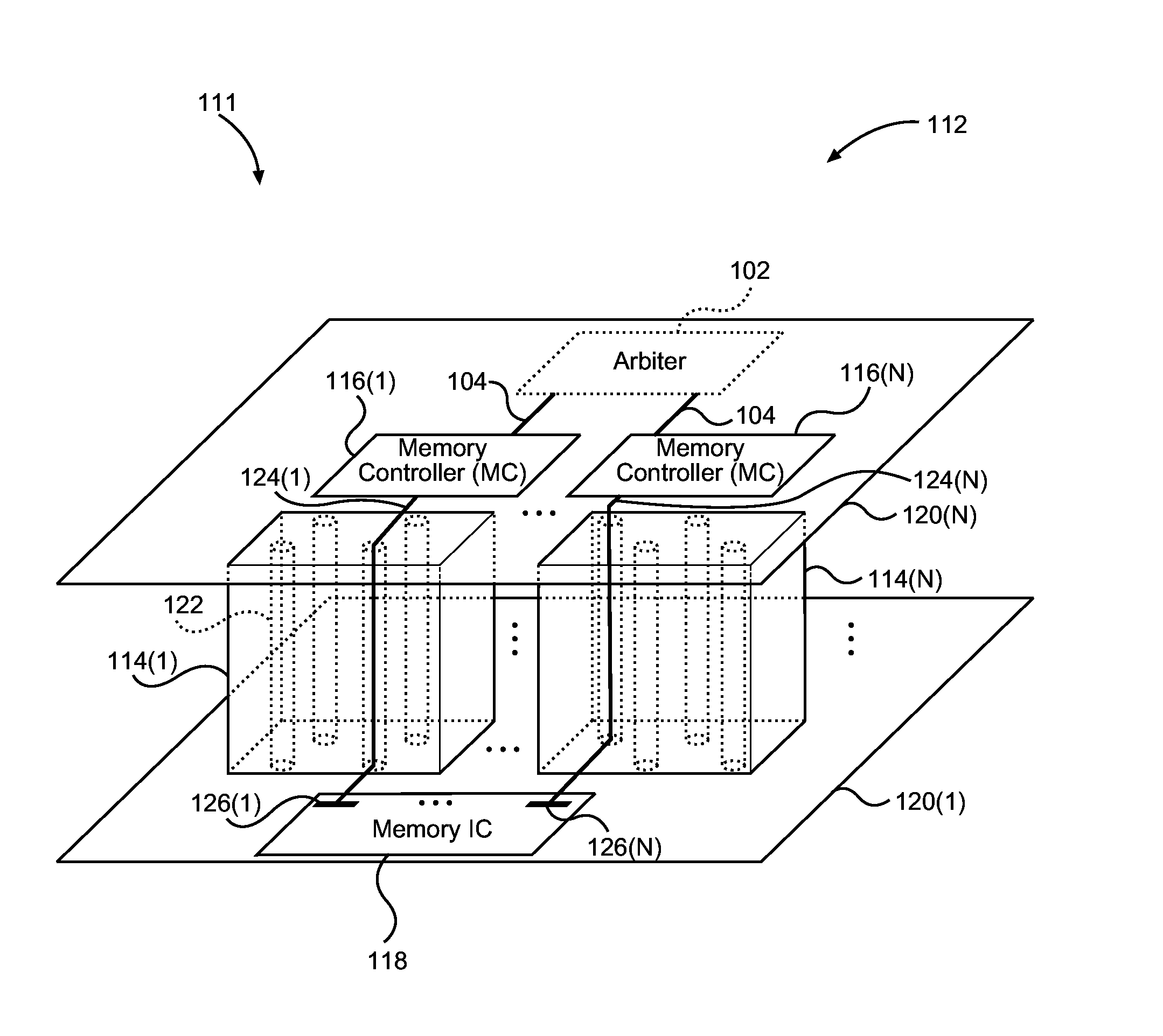
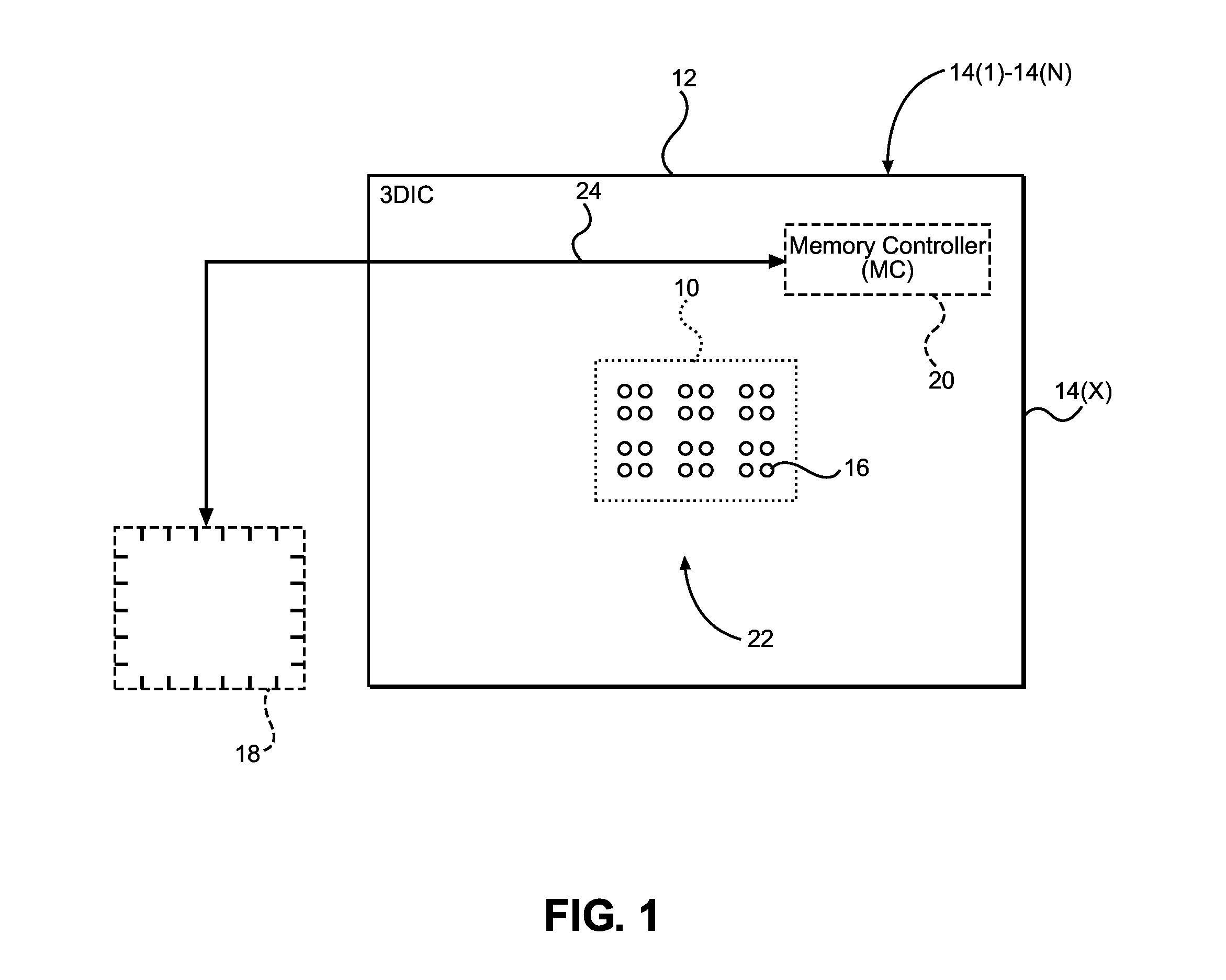
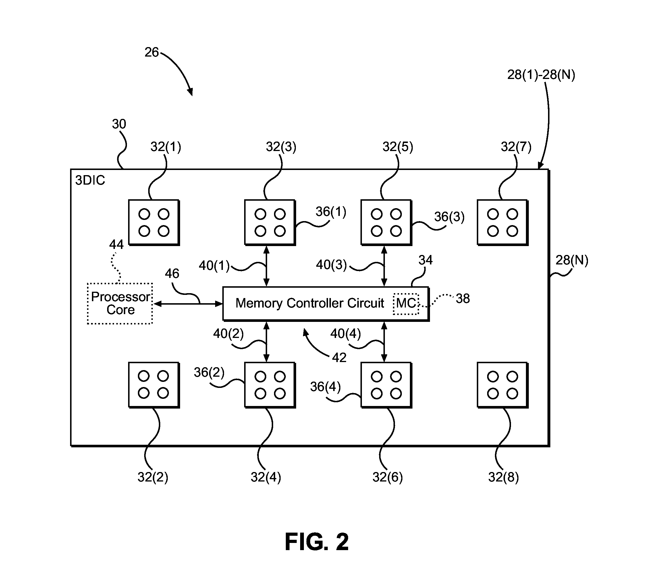
This patent is about how to place a memory controller in a 3D integrated circuit (3DIC) with distributed through-silicon-via (TSV) farms. The technical effect of providing distributed TSV farms is that it can improve performance, power, and area of the 3DIC, but it makes memory controller placement more challenging because it is desired to place the memory controller close to the TSV farm to minimize latency. The patent proposes a solution to this challenge by disclosing a method for placing the memory controller in the 3DIC based on a centralized placement scheme or a distributed placement scheme. By doing so, the memory controller can be placed close to multiple TSV farms while minimizing latency and avoiding complex intra-tier routing around a single centralized TSV farm.

Problems solved by technology

However, providing distributed TSV farms makes memory controller placement more challenging, because it is generally desired to place the memory controller as close as possible to the TSV farm to minimize latency of memory access requests from other tiers through the TSV farm to the memory controller.

Method used


Image

  • Memory controller placement in a three-dimensional (3D) integrated circuit (IC) (3DIC) employing distributed through-silicon-via (TSV) farms
  • Memory controller placement in a three-dimensional (3D) integrated circuit (IC) (3DIC) employing distributed through-silicon-via (TSV) farms
  • Memory controller placement in a three-dimensional (3D) integrated circuit (IC) (3DIC) employing distributed through-silicon-via (TSV) farms

Examples


Embodiment Construction

[0021]With reference now to the drawing figures, several exemplary aspects of the present disclosure are described. The word “exemplary” is used herein to mean “serving as an example, instance, or illustration.” Any aspect described herein as “exemplary” is not necessarily to be construed as preferred or advantageous over other aspects.

[0022]Aspects disclosed in the detailed description include memory controller placement in a three-dimensional (3D) integrated circuit (IC) (3DIC) employing distributed through-silicon-via (TSV) farms. The distributed TSV farms provide interconnections between circuits in different semiconductor IC tiers of the 3DIC. The 3DIC may be provided as a system-on-a chip (SOC) in which a memory system is provided in the 3DIC and accessed by other circuits, such as a central processing unit (CPU) or processor core, for data storage and retrieval. Providing distributed TSV farms in a 3DIC may achieve improved performance, power, and area (PPA) objectives and th...


PUM


Abstract

Aspects disclosed in the detailed description include memory controller placement in a three-dimensional (3D) integrated circuit (IC) (3DIC) employing distributed through-silicon-via (TSV) farms. In this regard, in one aspect, a memory controller is disposed in a 3DIC based on a centralized memory controller placement scheme within the distributed TSV farm. The memory controller can be placed at a geometric center within multiple TSV farms to provide an approximately equal wire-length between the memory controller and each of the multiple TSV farms. In another aspect, multiple memory controllers are provided in a 3DIC based on a distributed memory controller placement scheme, in which each of the multiple memory controllers is placed adjacent to a respective TSV farm among the multiple TSV farms. By disposing the memory controller(s) based on the centralized memory controller placement scheme and / or the distributed memory controller placement scheme in the 3DIC, latency of memory access requests is minimized.

Description

BACKGROUND[0001]I. Field of the Disclosure[0002]The technology of the disclosure relates generally to three-dimensional (3D) integrated circuits (ICs) (3DICs).[0003]II. Background[0004]Computing devices such as smartphones have become common in modem society. The prevalence of computing devices may be attributed to the many functions that are enabled within such computing devices. Increasingly complex integrated circuits (ICs) have been designed and manufactured to provide increasingly greater functionality in the computing devices. Concurrent with the increases in complexity of the ICs, there has been pressure to decrease footprint of the ICs. In a traditional two-dimensional (2D) IC (2DIC), all electrical components such as processor cores, memory chips, and logic circuits are disposed in a single semiconductor IC tier. Memory controllers are typically placed near input / output (I / O) pins of the memory chips to reduce memory access latency. However, as complexity of the IC grows, i...

Claims


Application Information

Patent Timeline
Patent Type & Authority Applications(United States)
IPC IPC(8): G06F13/16H01L25/065G06F13/42H01L25/00H01L23/50H01L23/48H01L25/18
CPCG06F13/1684H01L23/481H01L25/0657H01L25/18H01L2225/06544H01L23/50G06F13/4282G06F13/1605H01L25/50H01L27/0688H01L2225/06541H01L25/0652
Inventor LIM, SUNG KYUCHATHA, KARAMVIR SINGHDU, YANGSAMADI, KAMBIZ
Owner QUALCOMM INC
Learn More