Electrodeposition method for preparing polycrystalline copper having improved mechanical and physical properties
a technology of electrochemical and polycrystalline copper, which is applied in the direction of electrochemical coating, electrolytic coating, surface reaction electrolytic coating, etc., can solve the problems of component failure, premature and unpredictable service failure of normally ductile engineering materials,
- Summary
- Abstract
- Description
- Claims
- Application Information
AI Technical Summary
Problems solved by technology
Method used
Image
Examples
example 1
Outside Purity Window
[0061]2.3 mm thick free-standing plates of fine-grained copper precursor material were electroformed on a polished Ti cathode (150 cm2) in a conventional acid sulfate copper bath (60 I tank) containing 6000 molecular weight polyethylene glycol as a grain refiner and using phosphorized copper as the anode material. The plating current was supplied by a DYNANET™ PDPR 40-100-400 (Dynatronix, Amery, Wis., USA) pulse power supply. The electrolyte and the electroplating conditions used, along with chemical analysis data from the resultant electrodeposited material, are indicated in Table 2. A PHILIPS XL-30™ FEGSEM microscope in backscatter electron mode and equipped with TSL Orientation Imaging Microscopy (OIM) software version 5.0 was used to characterize the copper and the results are indicated in Table 3 below. The as-deposited average grain size of the electroformed copper was determined to be in the range of 800 to 900 nm. Individual specimens were then subjected...
example 2
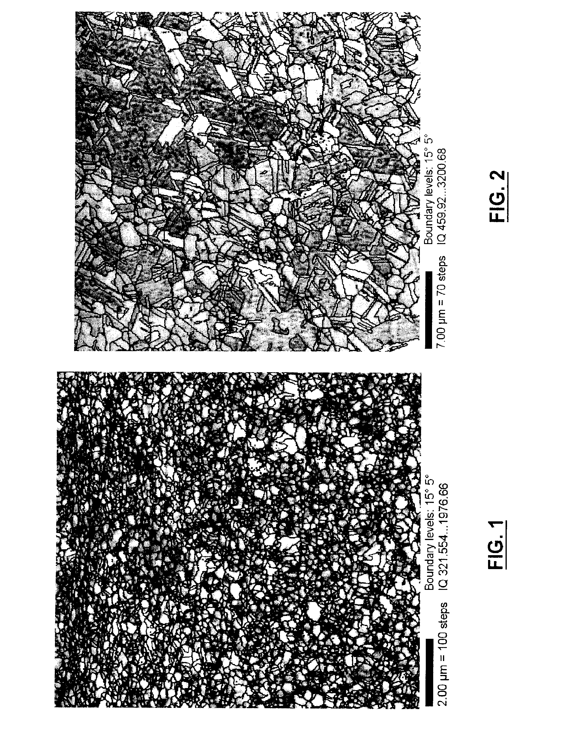
[0062]A 0.5 mm thick free-standing plate of fine-grained copper precursor material was electroformed on a polished Ti cathode (150 cm2) in a copper pyrophosphate-based bath (60 I tank) using OFHC copper as the anode material. The plating current was supplied by a DYNANET™ PDPR 40-100-400 (Dynatronix, Amery, Wis., USA) pulse power supply. The electrolyte and the electroplating conditions used are indicated in Table 4. Results of chemical assaying of this electrodeposited precursor material are also contained in Table 4. The evolution of the grain boundary character distribution, grain size, and preferred crystallographic orientation were evaluated using the same Orientation Imaging Microscopy (OIM) method described earlier and the results are indicated in Table 5 below. FIG. 1 is an OIM micrograph illustrating the pure copper microstructure immediately after electrodeposition. The as-deposited average grain size of the electroformed copper was determined to be in the range of 200 to ...
example 3
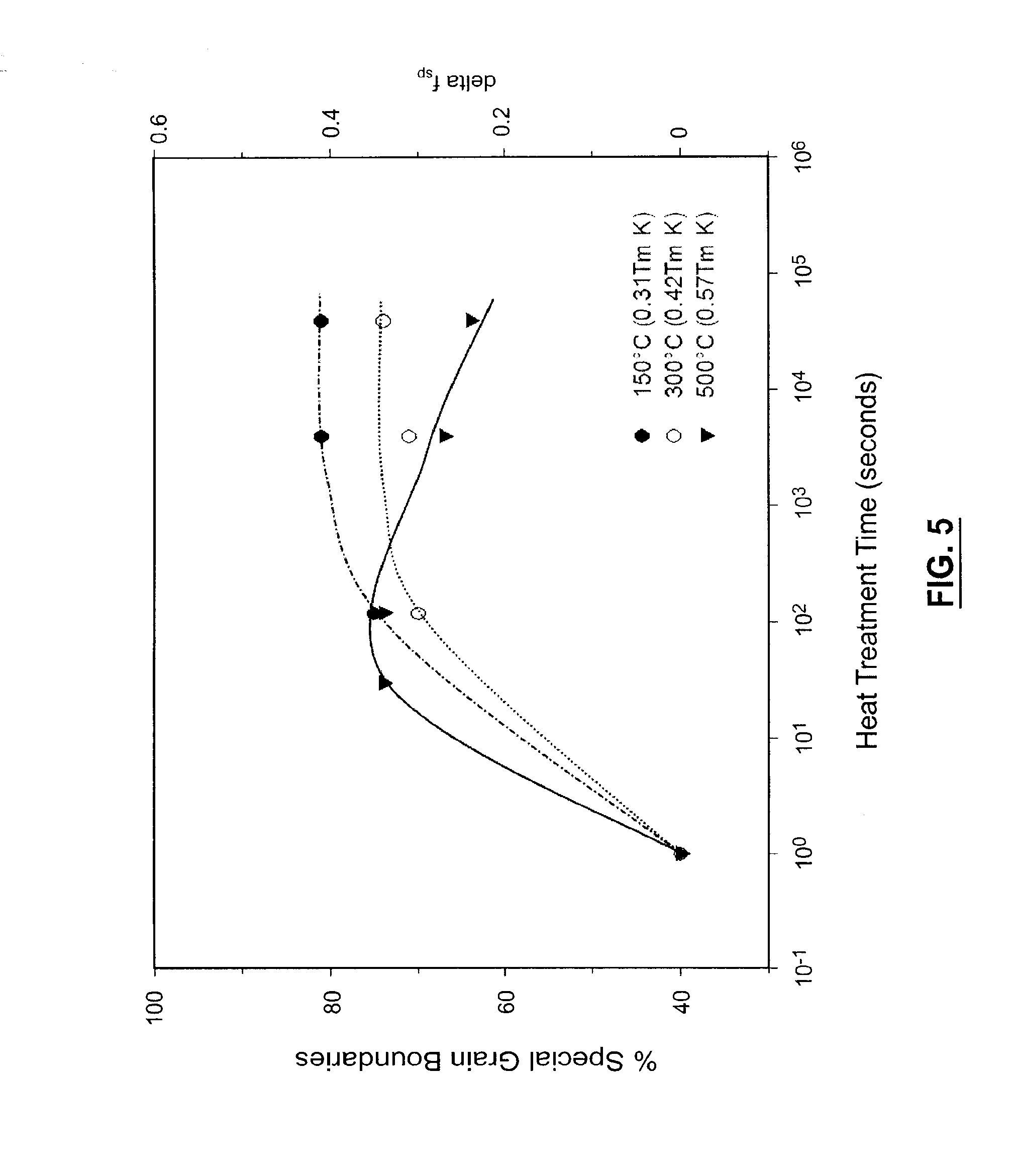
[0063]A 0.5 mm thick free-standing plate of fine-grained copper precursor material was electroformed in the same fashion to that described in Example 2. Chemical assay results of this material are shown in Table 6. The as-deposited average grain size of the electroformed copper was measured in Example 2 to be in the range of 200 to 400 nm and the ratio of thickness to grain size was determined in Example 2 to be in the range of 1250 to 2500. Because the materials were produced in the same fashion, the as plated grain size fsp and texture intensity value data for Example 2 is assumed to be the same for the present example. Individual specimens cut from this plate were then subjected to grain growth heat-treatments by immersion in molten salt at 150° C. (0.31 Tm, K), 300° C. (0.42 Tm K), and 500° C. (0.57 Tm K) for times ranging from 30 to 40,000 seconds. The evolution of the grain boundary character distribution, preferred crystallographic orientation and grain size were evaluated us...
PUM
| Property | Measurement | Unit |
|---|---|---|
| grain size | aaaaa | aaaaa |
| grain size | aaaaa | aaaaa |
| frequency | aaaaa | aaaaa |
Abstract
Description
Claims
Application Information
 - R&D
- Intellectual Property
- Life Sciences
- Materials
- Tech Scout
- Unparalleled Data Quality
- Higher Quality Content
- 60% Fewer Hallucinations
Browse by: Latest US Patents, China's latest patents, Technical Efficacy Thesaurus, Application Domain, Technology Topic, Popular Technical Reports.
© 2025 PatSnap. All rights reserved.Legal|Privacy policy|Modern Slavery Act Transparency Statement|Sitemap|About US| Contact US: help@patsnap.com


