Element manufacturing method and element manufacturing apparatus
- Summary
- Abstract
- Description
- Claims
- Application Information
AI Technical Summary
Benefits of technology
Problems solved by technology
Method used
Image
Examples
Embodiment Construction
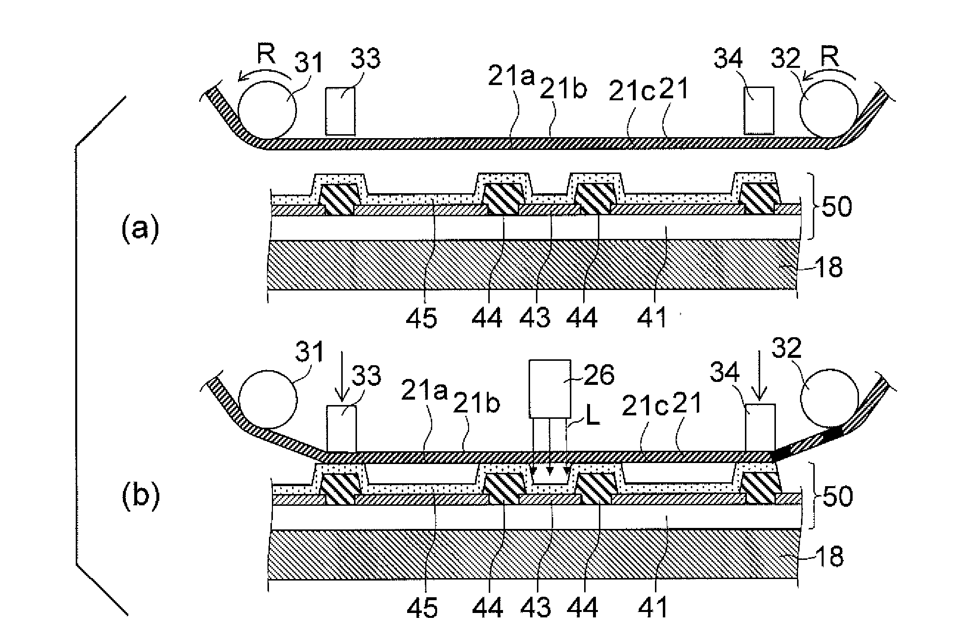
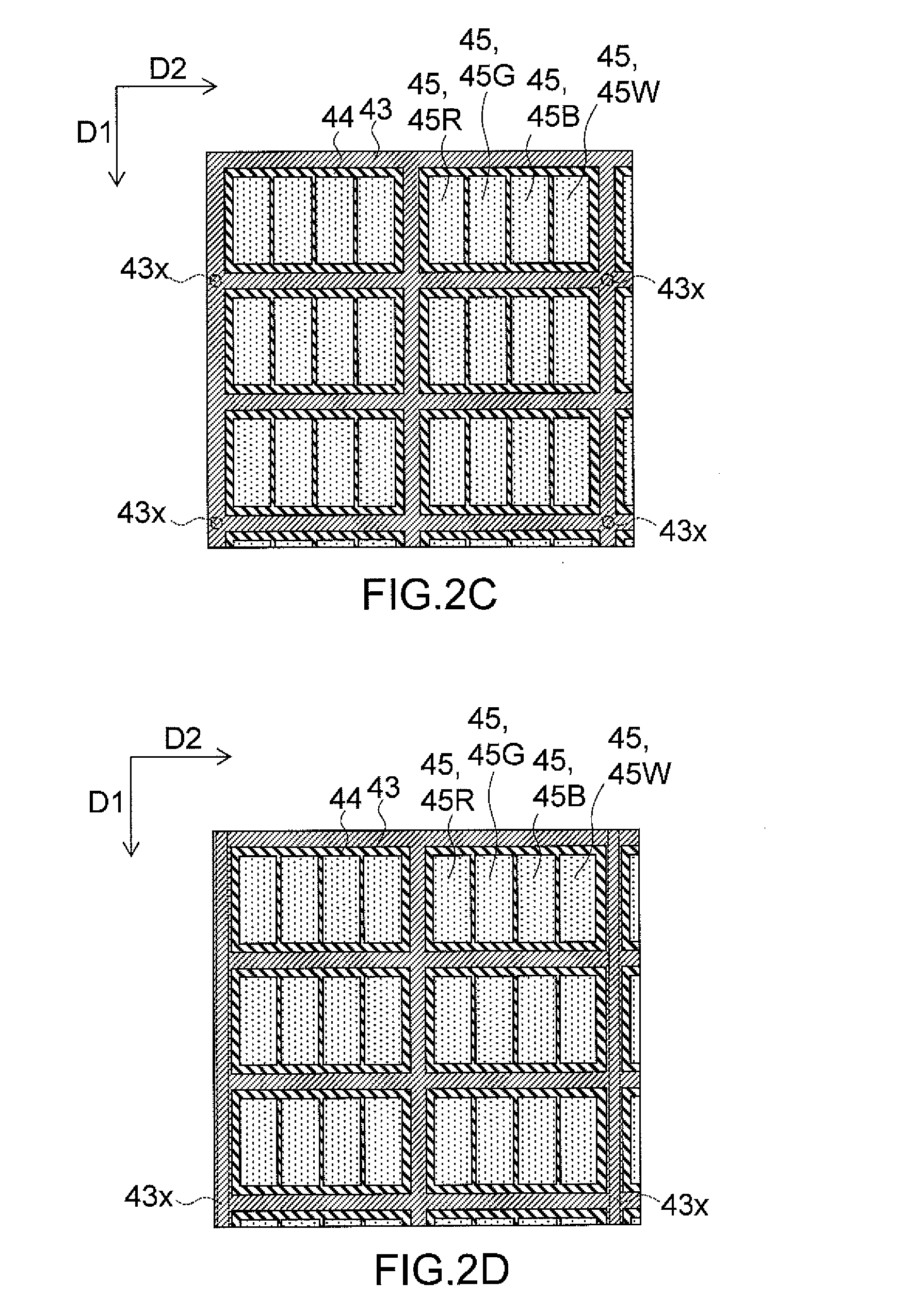
[0039]Hereunder, embodiments of the present invention will be described with reference to FIGS. 1 to 6. In the drawings accompanying the present Description, for the sake of illustration and easier understanding, scales, horizontal to vertical ratios, etc. are exaggeratingly modified from those of the real thing.
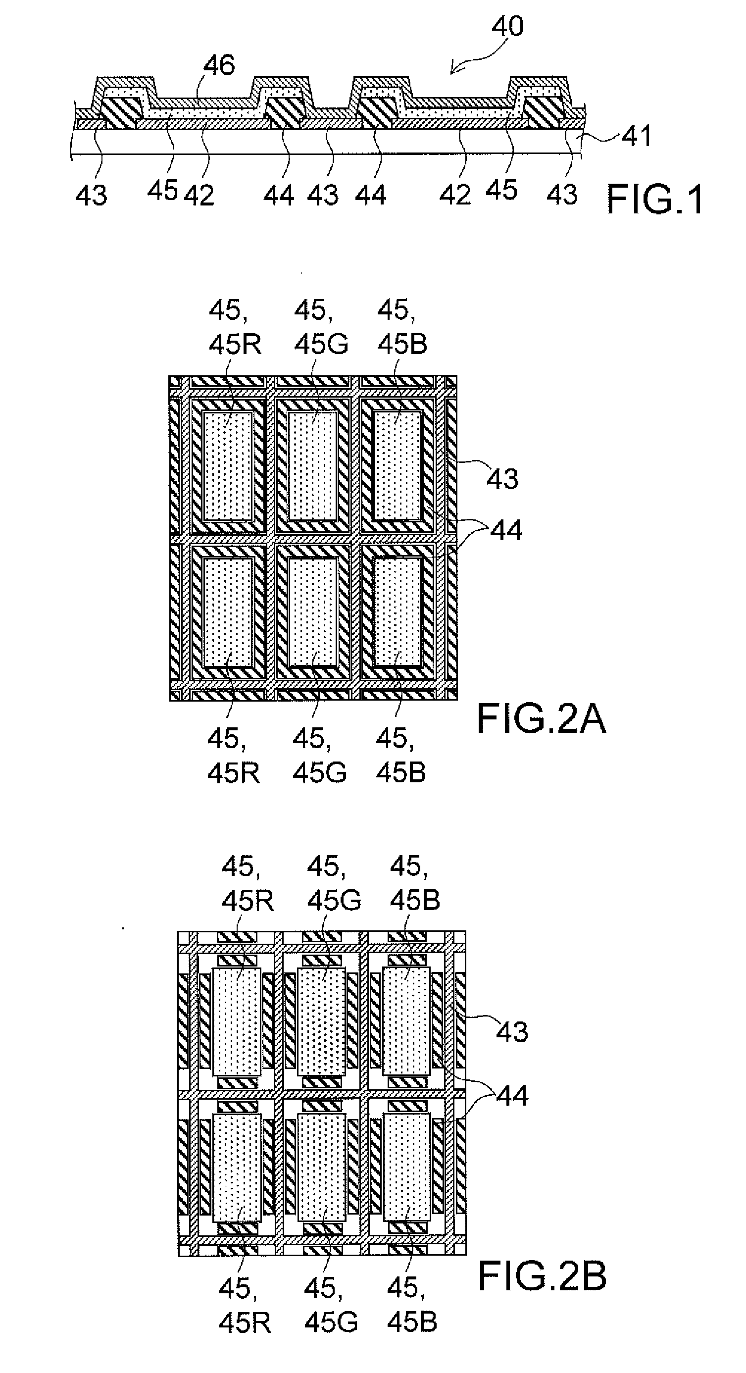
[0040]A layer configuration of an organic semiconductor element 40 according to an embodiment of the present invention will be first described with reference to FIG. 1. Here, a top-emission type of organic electroluminescent (EL) element will be described as an example of the organic semiconductor element 40.
Organic Semiconductor Element
[0041]As shown in FIG. 1, the organic semiconductor element 40 includes a substrate 41, a plurality of first electrodes 42 each disposed on the substrate 41, auxiliary electrodes 43 and protrusions 44 each disposed between any two of the first electrodes 42, organic semiconductor layers 45 each disposed on one of the first electrodes 42, and ...
PUM
| Property | Measurement | Unit |
|---|---|---|
| Thickness | aaaaa | aaaaa |
| Pressure | aaaaa | aaaaa |
| Magnetic field | aaaaa | aaaaa |
Abstract
Description
Claims
Application Information
 - R&D
- Intellectual Property
- Life Sciences
- Materials
- Tech Scout
- Unparalleled Data Quality
- Higher Quality Content
- 60% Fewer Hallucinations
Browse by: Latest US Patents, China's latest patents, Technical Efficacy Thesaurus, Application Domain, Technology Topic, Popular Technical Reports.
© 2025 PatSnap. All rights reserved.Legal|Privacy policy|Modern Slavery Act Transparency Statement|Sitemap|About US| Contact US: help@patsnap.com


